
In contrast, the millimeter-wave band still has a large number of potentially underutilized spectrum resources. Therefore, millimeter wave has become a research hotspot of the 5th generation mobile communication. The 5th generation mobile communication research alternative frequency bands were identified at WRC2015 in 2015: 24.25-27.5 GHz, 37-40.5 GHz, 42.5-43.5 GHz, 45.5-47 GHz, 47.2-50.2 GHz, 50.4-52.6 GHz, 66- 76 GHz and 81-86 GHz, of which 31.8-33.4 GHz, 40.5-42.5 GHz and 47-47.2 GHz are permitted as co-option bands under certain conditions of use. Various millimeter-wave devices, chips, and applications are in full swing. Millimeter waves have their own characteristics relative to the microwave frequency band. First, the millimeter wave has a shorter operating wavelength, which can effectively reduce the size of the device and system. Secondly, the millimeter wave has rich spectrum resources and can meet the needs of ultra-high-speed communication in the future. In addition, due to the short wavelength, millimeter waves have higher resolution for radar and imaging. So far, a lot of research has been carried out on millimeter waves, and various millimeter wave systems have been widely used. With the rapid development of civilian technologies such as the 5th generation mobile communication, auto driving, security inspection, etc., millimeter waves will be widely used in all aspects of people's daily lives.
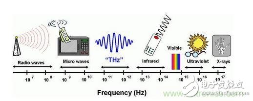
Millimeter wave
In terms of millimeter wave technology, combined with some popular system applications of millimeter wave band, such as millimeter wave communication, millimeter wave imaging and millimeter wave radar, the development of millimeter wave chips is highlighted.
1, millimeter wave chip
Conventional millimeter-wave monolithic integrated circuits mainly use compound semiconductor processes, such as gallium arsenide (GaAs) and indium phosphide (InP), which have good performance in the millimeter wave band and are the mainstream integrated circuit processes in this band. On the other hand, silicon-based (CMOS, SiGe, etc.) millimeter-wave sub-millimeter-wave integrated circuits have also made great progress in the past decade. In addition, high-power high-frequency devices based on gallium nitride (GaN) processes are rapidly expanding to the millimeter-wave band. The following will be introduced separately.
1.1 GaAs and InP millimeter wave chips
GaAs and InP processes and devices have made great strides in the last decade. Millimeter wave device types based on this type of process mainly include high electron mobility transistor (HEMT), modified high electron mobility transistor (mHEMT), and heterojunction bipolar transistor (HBT). At present, the cutoff frequency (ft) of GaAs, mHEMT, InP, HEMT and InP HBT exceeds 500 GHz, and the maximum oscillation frequency (fmax) exceeds 1 THz. In 2015, Northrop Grumman reported that the InP HEMT amplifier operating at 0.85 THz, 2013 In the United States, Teledyne and the California Institute of Technology's Jet Propulsion Laboratory reported an InP HBT amplifier operating at 0.67 THz. In 2012 and 2014, the Fraunhofer Institute for Solid State Physics in Germany reported an mHEMT amplifier operating at frequencies above 0.6 THz.
1.2 GaN millimeter wave chip
As a third-generation wide bandgap compound semiconductor, GaN has the advantages of large forbidden band width, high electron mobility and breakdown field strength. The device power density is more than 5 times that of GaAs, which can significantly increase the output power. Reduce size and cost. With the gradual maturity of GaN material preparation technology in the 1990s, GaN devices and circuits have become the hotspot in the development of compound semiconductor circuits. GaN is the focus of microwave and millimeter wave devices and circuits in the United States, Japan, and Europe. In the past decade, GaN's low-cost substrate material, silicon carbide (SiC), has also matured. Its lattice structure is matched with GaN and its thermal conductivity is good, which greatly accelerates the development of GaN devices and circuits. In recent years, GaN power devices have developed rapidly in the millimeter wave field. Japan's Eudyna reported a 0.15 m gate length device with a power output density of 13.7 W/mm at 30 GHz. The US HRL reported several E-band, W-band and G-band. The GaN-based device has a W-band power density of more than 2 W/mm and a power density of 296 mW/mm at 180 GHz. Domestic GaN power devices in the microwave band have matured, and GaN power devices in the W-band have also made progress. The Ka-band GaN power MMIC developed by Nanjing Electronics Research Institute has a pulse output power of 15W in the 3436 GHz band, an additional efficiency of 30%, and a power gain of more than 20 dB.
1.3 Silicon-based millimeter wave chip
Silicon-based processes have traditionally been dominated by digital circuits. With the continuous development of deep sub-micron and nano-processes, the silicon-based process features continue to decrease in size, and the shortening of the gate length compensates for the lack of electron mobility, thereby increasing the transistor's cutoff frequency and maximum oscillation frequency, which makes the silicon process Applications in the millimeter wave or even the terahertz band are possible. The InternaTIonal Technology Roadmap for Semiconductors predicts that the feature size of the CMOS process will be reduced to 5 nm by 2030, and the cutoff frequency ft will exceed 700 GHz. The cutoff frequency ft and maximum of the SiGe process transistors from the German IHP Institute The oscillation frequency fmax has reached 300 GHz and 500 GHz, respectively, and the corresponding silicon-based process circuit can be extended to more than 200 GHz.
Due to the huge advantages in cost and integration of silicon technology, the research of silicon-based millimeter-wave sub-millimeter-wave integrated circuits has become one of the current research hotspots. The University of Florida designed a 410 GHz CMOS oscillator. The University of Toronto, Canada developed a 170 GHz amplifier based on the SiGe HBT process, a 160 GHz mixer, and a 140 GHz CMOS-based inverter. The University of California, Santa Barbara, etc. The CMOS process developed a 150 GHz amplifier, and Cornell University developed a 480 GHz frequency multiplier based on a CMOS process. In terms of system integration, the University of Toronto designed the 140 GHz CMOS receiver chip and the 165 GHz SiGe on-chip transceiver system. The University of California, Berkeley, first integrated the 60 GHz band silicon-based analog transceiver circuit with digital baseband processing circuitry. On the CMOS chip, the Singapore Microelectronics Research Institute also implemented a 60 GHz CMOS transceiver chip including a chip antenna. The University of California, Los Angeles reported a frequency synthesizer of 0.54 THz. The Upattal University of Germany developed 820 GHz. The silicon-based SiGe active imaging system, the University of California at Berkeley, successfully developed the 380 GHz radar system using the SiGe process. Japan's NICT and other CMOS-based CMOS processes have implemented 300 GHz transceiver chips and achieved transmission rates in excess of 10 Gbps, but because of the lack of power amplification and low-noise circuitry, the transmission distance is very short. By using silicon-based technology, all circuits including digital circuits can be integrated on a single chip, which is expected to significantly reduce the cost of millimeter-wave communication systems.
In the case of millimeter-wave submillimeter-wave silicon-based integrated circuits, China has started late, but with the support of the National 973 Program, the 863 Program, and the Natural Science Foundation, research has been rapidly carried out and progress has been made. The National Key Laboratory of Millimeter Waves of Southeast University successfully designed Q, V and W band amplifiers, mixers, VCOs and W-band receivers, Q-band multi-channel transceivers, etc., and to 200 GHz based on 90 nm CMOS technology. CMOS multiplier and SiGe oscillator to 520 GHz.
2, millimeter wave electric vacuum device
Millimeter wave integrated circuits have many advantages such as small size and low cost, but power is limited. In order to obtain higher output power, electric vacuum devices can be used. For example, the Klystron developed by CPI of Canada has obtained more than 2000 W pulse output power in the W band. The traveling wave tube developed by Beijing Institute of Vacuum Electronics (TWT) The pulse output power of the amplifier in the W band exceeds 100 W. The University of Electronic Science and Technology has also successfully designed the TWT power amplifier in the W band. The Gyrotron developed by the Hefei Institute of Material Science, Chinese Academy of Sciences was obtained at 140 GHz. The pulse output power of 0.9 MW is equivalent to the foreign level.
3, millimeter wave application
In recent years, the performance of millimeter wave devices has been continuously improved, and the cost has been continuously reduced, which has greatly promoted the application of millimeter waves in various fields. At present, applications based on the millimeter wave band are mainly embodied in millimeter wave communication, millimeter wave imaging, and millimeter wave radar.
3.1 millimeter wave communication
With the rapid development of wireless communication technology, the spectrum of the gold communication band below 6 GHz is already very crowded, and it is difficult to meet the demand for wireless high-speed communication in the future. However, in contrast, in the millimeter-wave band, the spectrum is rich in resources but still not fully exploited.
In the field of mobile communication, the millimeter wave mobile communication system scene, network structure and air interface are explored. In the current 5th generation mobile communication (5G) study, several millimeter wave bands have become 5G candidate bands. Millimeter wave technology will play a pivotal role in the development of 5G.
In the short-range high-speed communication system, the 60 GHz band has been extensively studied and applied. Free spectrum resources in this band have been opened in Europe, the United States, Canada, South Korea, Japan, Australia and China. The 60 GHz band is at atmospheric attenuation peaks, although it is not suitable for long-distance communication, it can be used for short-distance transmission without causing too much interference to the surroundings. In recent years, various systems and standards such as high-speed Gbps communication, WirelessHD, WiGig, near field communication, IEEE 802.11ad, and IEEE802.15.3c have been developed in the 60 GHz band.
The Southeast University of China has proposed the ultra-high-speed near-distance wireless transmission standard (Q-LINKPAN) working in the 45 GHz band, and its short-range part has become the IEEE 802.11aj international standard. At 45 GHz, the atmospheric attenuation is less than 1 dB/km, so it can not only achieve high-speed short-distance transmission like the 60 GHz band, but also for long-distance transmission. At present, the experimental system has achieved a transmission rate of 2 Gbps at a transmission distance of 82 m, and has developed a corresponding millimeter wave chip supporting Gbps transmission.
Satellite communication covers a wide range and is an important means to ensure remote areas and maritime communications and emergency communications. At present, its working frequency bands are mainly concentrated in the L, S, C, Ku and Ka bands. With the deepening of satellite communication research, higher frequency bands have been tried. Because the millimeter wave band can provide a wider bandwidth, a higher communication rate can be achieved. In addition, low power consumption, small size, anti-interference and high spatial resolution are all worthwhile. At present, the main research directions of satellite and terrestrial communication are concentrated in two windows with less atmospheric attenuation, Q-band and W-band, and the 60 GHz band is considered to be an important frequency band for inter-satellite communication.
In addition, the millimeter wave optical-borne wireless communication (RoF) system has also been rapidly developed. Optical fiber has the advantages of low cost, large channel bandwidth, low loss, strong anti-interference ability, etc., and has become an indispensable part of modern communication systems. As mentioned above, the millimeter wave has the advantages of large transmission capacity, small volume, and the like, but also has disadvantages such as large space transmission loss. The millimeter-wave RoF system combines the advantages of millimeter-wave and fiber-optic communication, and is an effective means to achieve long-distance transmission of broadband millimeter-wave communication. Since the concept of optical wireless communication was proposed in 1990, this field has become a research hotspot in the millimeter wave band. Many research groups have studied in different millimeter wave bands, such as 60 GHz, 75-110 GHz, 120 GHz, 220 GHz, 250 GHz, etc.
3.2 millimeter wave imaging
Using the advantages of millimeter wave penetration and safety, millimeter wave imaging can effectively image the detected object, and has been widely studied in national security, airport security, atmospheric remote sensing, etc. According to the imaging mechanism, it is divided into passive imaging and Active imaging. Millimeter wave passive imaging is achieved by detecting the radiant energy of the measured object itself and distinguishing the difference in radiation intensity of different substances. Passive imaging is a safe imaging method that does not cause electromagnetic interference to the environment, but requires high intensity of the signal itself and sensitivity of the receiver. A large amount of research has been carried out on millimeter wave passive imaging technology at home and abroad.
The millimeter wave active imaging mainly emits a millimeter wave signal of a certain intensity through a millimeter wave source, and detects the difference between the measured object and the environment by receiving the reflected wave of the measured object, and then performs inversion imaging. Active imaging systems can detect non-metallic objects, including plastics, which are less affected by the environment and have a large amount of information that can be efficiently imaged in three dimensions. Commonly used active imaging systems mainly include focal plane imaging and synthetic aperture imaging. The millimeter wave imaging system has been applied to the security inspection of many airports at home and abroad. The Sun Xiaoyu team of the Shanghai Institute of Microsystems has successfully developed a millimeter-wave imaging security inspection system. The team of Fan Yong of the University of Electronic Science and Technology has successfully developed a millimeter-wave dynamic imaging system.
3.3 mm wave radar
Millimeter wave radar has the characteristics of frequency bandwidth, short wavelength, narrow beam, small size, low power consumption and strong penetrability. Compared with laser infrared detection, its strong penetrability ensures that the radar can work in fog, rain, snow and dust, and is less affected by the weather. Compared with the radar in the microwave band, the use of the short wavelength of the millimeter wave can effectively reduce the system volume and weight and improve the resolution. These characteristics make the millimeter wave radar have important applications in car collision avoidance, helicopter obstacle avoidance, cloud detection, and missile guidance.
Microwave millimeter-wave anti-collision radars are mainly concentrated in the 24 GHz and 77 GHz bands and are one of the core technologies for smart driving or autonomous driving in the future. In the research of helicopter millimeter wave anti-collision radar, people pay special attention to the detection effect of millimeter wave radar on power lines.
Millimeter waves also have important applications in atmospheric remote sensing, and representative ones are millimeter-wave cloud radars. The millimeter wave cloud radar is mainly used for detecting precipitation clouds, and is used to detect macroscopic and microscopic parameters inside the cloud, reflecting atmospheric thermal and dynamic processes. Due to the short wavelength of the millimeter wave, it exhibits high measurement accuracy and resolution in cloud detection, and has the advantage of penetrating thick clouds with more water. The team of Ge Junxiang of Nanjing University of Information Science and Technology developed the W-band cloud radar. The Lu Wei team of Beijing Institute of Technology is developing a 94/340 GHz dual-band cloud radar.
In addition to civilian use, millimeter-wave radars also have very important applications in military applications. For example, in precision-guided weapons, millimeter-wave radar guidance is a core technology and an effective means of achieving targeted precision strikes around the clock.
Correct Electronic Calculator advantage:
14 digits tax calculator,check calculator,We use good quality LCD display screen.fonts are clearly visible.Dual power solar power make life recycling.With the first raw material, fine workmanship and repeated testing, ABS is more durable and firm.

Correct Electronic Calculator,Correct Calculator,Correct Scientific Calculator,Check Correct Function Calculator
Dongguan City Leya Electronic Technology Co. Ltd , https://www.dgleya.com