
With the extensive application of the Internet of Things in the national economy, such as smart grid, intelligent transportation, intelligent logistics and ecological monitoring, the RFID technology in the UHF band is developing rapidly. It is a non-contact automatic identification technology that can be automatically transmitted through RF signals. Identify target objects, obtain relevant data, identify work without manual intervention, and apply to all kinds of harsh environments. The RFID system consists of three parts: the tag, the reader and the antenna. Among them, the RFID reader is the most critical.
1 system design
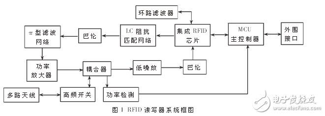
The long-range RFID reader system based on the AS3992 chip mainly includes a radio frequency portion and a baseband portion, as shown in FIG. The RF part is designed around the RFID integrated chip AS3992. The loop filter works with the built-in VCO to generate accurate frequencies. The transmit link is mainly composed of balun, power amplifier, coupler, high frequency switch and multi-channel antenna interface. It is used on critical paths. The LC network and the π-type network adjust impedance matching; the RF receiving link consists of an antenna, a high frequency switch, a coupler, a low noise amplifier, and a balun. The baseband section is equipped with an upgradeable MCU host controller and a common peripheral interface.
2 hardware circuit design
2.1 AS3992 and its peripheral circuits
The AS3992 is a high-performance UHF-band reader chip from austriamicrosystems that integrates analog front ends such as mixers, gain filters, voltage-controlled oscillators, phase-locked loops, and analog-to-digital/digital-to-analog converters. And built a complete protocol processing system ISO18000-6C. The external controller only needs to pass the 8-bit parallel port or SPI port to achieve all communication and control of the AS3992.
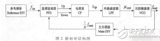
The UHF carrier signal has a communication frequency of 840 MHz to 960 MHz. The AS3992 integrates a VCO, a prescaler, a main divider, a reference divider, a phase detector, and a charge pump. The peripheral circuit can be composed of a loop filter. A complete phase-locked loop (PLL) circuit, as shown in Figure 2. The output frequency of the PLL is determined by the product of the reference divider and the product of the main divider. The main function of the charge pump (CP) is to convert digital logic pulses into analog currents. The CP signal is fed back to the VCO pin via a low-pass filter to adjust the oscillator frequency accuracy. In order to obtain a stable VCO tuning voltage, an external loop filter circuit is particularly important to maintain loop stability, control loop noise inside and outside the loop, prevent voltage abrupt changes on the VCO tuning voltage control line, and suppress reference sideband spurious interference. And so on.
2.2 RF transmitting circuit
The AS3992 chip RF signal is output as a differential pair. The LC impedance matching network can be used to accurately match the balun's input impedance to 100Ω, and a single-ended UHF signal can be output through a 2:1 balun. If only the AS3992 internal power amplifier is used, its output power is only 20 dBm at most, which can only satisfy short-distance reading and writing. To achieve farther read/write distance, distortion-free amplification must be performed by an external power amplifier; also for impedance matching of the entire RF line, a π-type filter network is placed between the balun and the amplifier for impedance trimming.
The power amplifier can power amplify the already modulated high frequency carrier signal, radiate it around the antenna to meet the intensity of the excitation electromagnetic field required by the receiver, and have no effect on adjacent channels. The power chip SKY65111 uses three-stage voltage control with a 1 dB compression point gain of 29.5 dBm. Using the AS3992's own DAC, the voltage follower can be used to easily and accurately adjust the output power of the amplifier; in addition, when the external amplifier is fixed, it is transmitted by the AS3992 itself. The power adjustment can also be adapted to different distance applications.
The isolation of the microwave signal input/output needs to pass through the coupler, and the signal from the coupler enters the one-fourth high-frequency switch SKY14151, and one signal can be switched to any selected antenna interface according to the application requirements. The four antenna interfaces designed by the reader not only extend the application distance, but also because a reader can have multiple sub-nodes to send and receive information. When four antennas are aligned in the same direction, the single-segment can also reduce the single The dead zone of the antenna reduces the bit error rate.
In order to increase the maximum distance of the RFID reader, it is also necessary to detect its transmission power. If the transmission power is too large, it will not only cause distortion, but also leak to the receiving end to form interference. Therefore, once the power detection device monitors more than the set power, the fine tuning amount is loaded to the power chip SKY65111 through the digital PID and DAC of the main controller. The stage voltage control terminal makes the transmission power controllable.
2.3 RF receiving circuit
The RF receiving circuit based on the AS3992 chip is relatively simple, because it integrates the mixer and filter inside the AS3992 chip, and the peripheral circuit only needs to add a 1:2 balun to convert the single-ended signal into a differential pair signal. , the RF receiving pin that is sent to the AS3992 chip. In order to reduce the clutter interference and improve the purity of the RF receiving signal, a low noise amplifier is added between the coupler and the balun, so that the balun input signal is limited to 840 MHz~960 MHz.
3 software programming
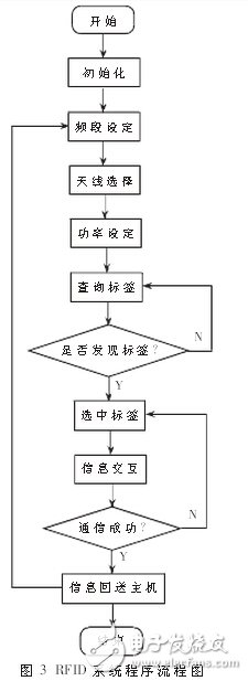
The firmware program of the AS3992 is written in the MCU main controller. Connect the RFID system to the computer through the peripheral interface. After power-on, first initialize the AS3992 chip; after successful, you can set the frequency band, antenna interface and output power (the frequency band selection depends on national standards, the antenna interface can be switched according to needs, output The size of the power usually determines the distance between the read and write distances; the main control triggers the query tag action. If there is a tag in the effective range of the antenna radiation, the tag is selected for communication, otherwise the query is repeated; after the main controller and the tag communicate with each other successfully , the tag information is sent back to the host computer to complete a card reading operation. The system program flow chart is shown in Figure 3.
4 system test
The performance of the designed RFID system is tested using a spectrum analyzer. The emission spectrum of the antenna interface is shown in Figure 4. The maximum transmit power is 27 dBm. When the transmit power is set at 15 dBm, from the emission spectrum as shown in Figure 5. It can be seen that the channel power is 14.31 dBm and the occupied bandwidth (99% energy) is 119 kHz.
This paper designs a long-distance RFID modular system based on UHF band. As data transmission and resolution requirements increase, MCU master controllers can be continuously upgraded to accommodate transaction control expansion and processing speed. The design of the output power detection can prevent the problem of blindly increasing the transmission power and causing the reception interference to affect the recognition distance. At present, the system has been successfully applied to the positioning of Baosteel's hot-rolled circular rail transport vehicles.
The solar power supply system USES photovoltaic cells to convert solar energy into electricity, which is used to power electrical appliances and batteries by stabilizing the system. The voltage of the photocell output is too large for light, so it must be stabilized before it can be used. Cell phone battery storage is ok, but consider the voltage and capacity of the battery.Anti-reflective Coated glass along with UV-T UV-C encapsulant ensure higher transmission efficiency. •Higher efficiency cells (+18%) for more power output •Positive power output tolerance (+5%) •PID resistant Cells encapsulants yield efficient performance under hot humid weather. •Resistant to salt mist corrosion. •IP65 / IP67 rated junction box with 3, 25 A diodes, giving 15A box rating. •Certified for 1500 V system voltage .
Poly 150W Solar Panel,150W Solar Panel,150 Watt Solar Panel
Yangzhou Bright Solar Solutions Co., Ltd. , https://www.solarlights.pl