
Many applications, from frequency counting and synthesis to sensor signal conditioning, require the conversion of RF signals to digital logic levels. Under these circumstances, designers generally use a high-speed voltage comparator to complete the conversion of RF to digital signals. Since voltage comparators have high gains, they generally have good sensitivity, but they also pose problems. High-speed comparators are expensive, and it is difficult to find ready-made products and they are easily eliminated.
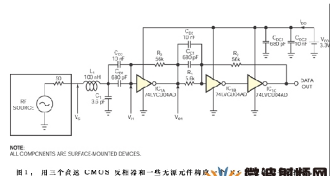
The circuit in Figure 1 can provide an attractive solution for frequencies up to 180 MHz. The IC in the design is a 74LVCU04 high-speed CMOS inverter. It can be either off-the-shelf or from many sources. In addition, many devices may already contain three unused inverters. An inverter IC1A works as a linear preamplifier to form the input stage of the converter. The bias resistor R3 averages the inverter's input and output voltages at half the supply voltage [VO1 = VI1 = (VDD/2)], allowing the inverter to enter its own linear region. Since the AC gain of the very high speed CMOS inverter is relatively low on the RF stage, (VO1/ VI1)≈7, a gain stage is added after the preamplifier. The added inverter cascade scheme is not stable at low frequencies and DC when no RF signal source is applied.
The circuit in Figure 1 solves this problem using a topology based on Schmitt triggers and amplifier circuits (IC1B and IC1C), which includes a frequency-dependent positive feedback network consisting of R1, R2, CD1, and CD2 composition. With different input frequencies, the network can exhibit two characteristics: At high frequencies, the decoupling capacitor shorts feedback resistor R1 to CDC1 and CDC2, thereby canceling out the positive feedback networks R1, R2 and inverter IC1B. Input capacitance caused by the time constant. Therefore, at high frequencies, the three inverters IC1A, IC1B, and IC1C appear as three cascaded high-speed amplifiers to achieve the best input signal bandwidth. At DC and low frequencies, the effect of the coupling capacitor on CD1 and CD2 is negligible, and the inverter IC1B, IC1C and the positive feedback network R1, R2 can function as a Schmitt trigger circuit. In order to make a trade-off between the input sensitivity of the VS and ensuring unconditional stability of the comparator output, a choice is made between the high and low threshold voltages VTH and VTL at the Schmitt trigger input VO1. Equations 1 and 2 set the high and low threshold voltages:
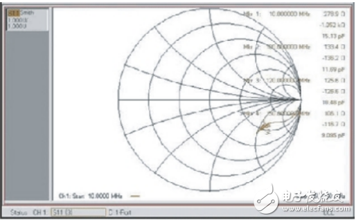
To neutralize the problem of sensitivity degradation at higher frequencies, a low-Q impedance matching network consisting of L1 and C1 is added to the input of the comparator. Since the design goal is to obtain acceptable sensitivity up to 160 MHz, the network matches the 50Ω RF source with the input impedance ZI1 of IC1A running at 150 MHz. Unfortunately, manufacturers of digital ICs often do not account for the input impedance of logic devices. Therefore, when designing the matching network, the first task is to measure the scattering parameter S11 at the input VI1 of the first inverter IC1A with an Agilent vector network analyzer. Figure 2 shows the Smith Chart of the inverter S11 parameters.
A known
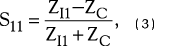
Where ZC = 50Ω, the input impedance of the first inverter at the desired frequency can be extracted using the data in FIG. 2 . At 150 MHz, ZI1 = 106.1 Ω-j 116.7 Ω is obtained (at the mark 4 in FIG. 2 ). To determine the value of each component in the matching network, you can use any software tool (References 1 and 2). If you are not familiar with the calculation of the Smith chart, you can also use the following methods for analysis:
1. Using the series-parallel conversion formulas (Equations 4 and 5), convert the input impedance of the first inverter to parallel:
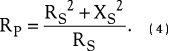
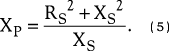
Using these formulas for 150 MHz results in: RP=233Ω, XP=213Ω. (At 150 MHz, XP stands for input impedance, CP = 5 pF.)
2. Calculate the initial value of the network match between the first inverter input impedance RP and the 50Ω RF source. Use Equations 6 and 7 to calculate the values ​​of the components in the matching network (Reference 3).
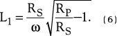
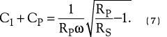
Using these formulas for 150 MHz yields L1≈100 nH and C1 +CP≈8.7 pF.
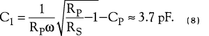
3. Subtract the inverter's input capacitance CP = 5 pF from Equation 7, and calculate the value of C1:
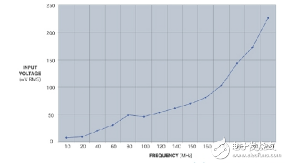
When building the circuit, use the standard components closest to the calculated values: L1=100 nH, C1=3.6 pF. As shown in the input frequency vs. sensitivity curve in Figure 3, the sensitivity of the circuit increases from 100 MHz to 170 MHz, which clearly demonstrates the effectiveness of the impedance matching network. This method can be applied to any other frequency band of interest at the selected frequency to optimize circuit sensitivity. In the range of input signals from 10 MHz to 180 MHz, the power consumption of the RF-to-digital logic converter does not change much. In the worst case, the current consumed by the 3.3V supply does not exceed 58 mA.
IJOY Vape,IJOY E-Cigarette,IJOY Disposable Vape,IJOY Vape Kit,IJOY Vape Pod
TSVAPE Wholesale/OEM/ODM , https://www.tsecigarette.com