
As electronic products become more compact, more powerful, and more versatile, the ultimate system-level requirements, as well as the complexity of mobile and stationary devices, are becoming increasingly prominent. This complexity stems from the requirement to implement wireless and wired interconnections between analog and digital circuits, requiring system engineers to use multiple power rails and hybrid circuit designs. Circuits with analog and digital signals tend to have several ground references, which often leads to cluttered circuits, unachievable design goals, and seemingly reliable solutions that ultimately become the source of failure. The focus here is on understanding the needs of the circuit and pre-planning the final system, as the result of these two steps is effectively turning the drawing into the final printed circuit board. Take some time in the design phase to consider each functional block of a complex system from the perspective of current path and noise sensitivity, and then set up these modules and power supply circuits based on simple axioms in which current always flows in a loop, so that today The complex circuits that system engineers face can be broken down into many manageable parts for the ultimate reliable design.
Power and ground analysis of simple circuits
To prove the theory, let's look at a simple circuit and consider the connections shown. The basic circuit consists of three elements, a low dropout (LDO) linear regulator, a microprocessor USB cable connected to the audio driver, and a speaker, all powered by a USB plug connected to a computing host. In this example, the USB to audio driver must be powered from 3.3V. Since the speakers are powered by the output of the audio driver, the audio input driver requires +3.3V LDO, which is powered by the USB connector (+5V), which seems to give an obvious conclusion that they can be placed in Figure 1(a) The position shown in the schematic. However, in this framework, the current that drives the speaker's operation will produce a voltage bounce when returning to the current source driver, which will in turn act on the LDO and ultimately affect the USB connector. In this example, the reference voltage that converts USB data to music bounces at the rate of music playback. The phase shift due to the speaker inductance increases the error, which is mixed with the high volume due to the current boost. Voltage bounce will also cause ripple to appear, which will reduce the sound quality of the speaker.
This will reduce the ripple reaching the DC, after which the current will only cause a voltage drop and will not change much over time (Δt in the above equation should be considered as the average of the audible frequency 12~14kHz). The magnitude of the error can be controlled by limiting the voltage drop (the product of current and resistance) obtained by Ohm's law by using a wider power supply and GND connection between the ICs.
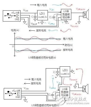
Figure 1: A simple circuit shows that the power circuit will cause a bounce and will return to the power supply.
The width of the GND and power lines should be determined based on acceptable losses. For a typical 1 ounce copper printed circuit board, the resistance can be estimated to be approximately 0.5 mΩ per square. Since this problem cannot always be alleviated by adding a capacitor, it should be solved fundamentally using the scheme in Figure 1(b). The LDO is placed above the audio driver IC, which allows the stereo current loop to avoid sensitive audio drive GND, so that the resulting GND voltage bounce does not affect the audio drive, only small ripple interference occurs.
Power and Ground Optimization Strategies for Complex Circuits
In the above application case, there are only two current loops. Now let's change to a more complicated example. The next consideration is a more complex tablet system. In this example, the tablet includes a backlight, a touch screen, a camera, a charging system (USB and wireless), Bluetooth, WiFi, audio output (speakers, headphones), and a memory for storing data. Of course, most of these applications require power rails of different voltages to work better. As shown in Figure 2, the system has five power rails and two methods of charging the battery, which means there are at least five current loops. However, compared with DC power supplies and related current paths, there are more aspects to consider in practical applications. There are multiple switching regulators in the circuit, broadcast and receive antenna systems, all of which require the use of a microprocessor for coordination and control. The power and GND paths shown in the power supply and the modules they power on help to summarize power and load current evaluations for the following purposes:
In Figure 2, the main power rail has been color coded and the current flowing through the corresponding GND symbol has been matched to the supply rail that supplies the current. For example, every component (red) that is not related to battery charging has a terminal current returning to the battery, but the USB to audio IC is powered by a 3.3V BUCK regulator, which is powered by a 5V Boost regulator and then received battery. Therefore, the GND current is returned from the audio IC to each regulator in sequence, and then reaches the battery, and the audio IC current does not directly return to the battery.
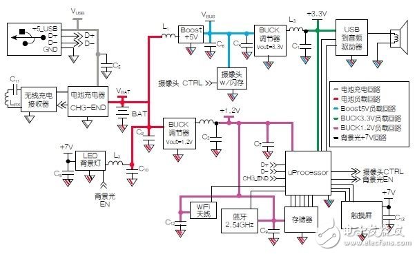
Figure 2: Typical mobile tablet schematic module.
The system shown in Figure 2 uses a lithium-ion battery that can be charged via a USB charger or wireless power transmitter and receiver. The battery voltage can be boosted to +5V (for camera zoom motors, +3.3V buck regulators for microprocessors, audio and touch screens), stepping down to +1.2V (for microprocessors, memory, Bluetooth and WiFi) can also be boosted to +7V for camera flash. Obviously, voltage regulators should be placed near their respective loads, but ultimately, due to product size limitations, designers are often forced to place the load farther away from the power supply or to mix it around the board. It can be seen that each power supply needs to support multiple loads, so careful routing and layout schemes must be used to control current paths and unintentional EMI. Here are some important layout considerations: i) available space, ii) mechanical constraints, iii) acceptable voltage drop for power and GND rails (product current and number of traces/plane squares), iv) power supply And GND current path, as well as v) cost (PCB layer, component), vi) the frequency of the digital or analog signal, and the feasibility of returning the path directly from the power supply.
As a final case, here is a hypothetical final system with mechanical constraints. In such systems, the user interface and overall size can impose some limitations on the design. Figure 3 shows the actual location of each module:
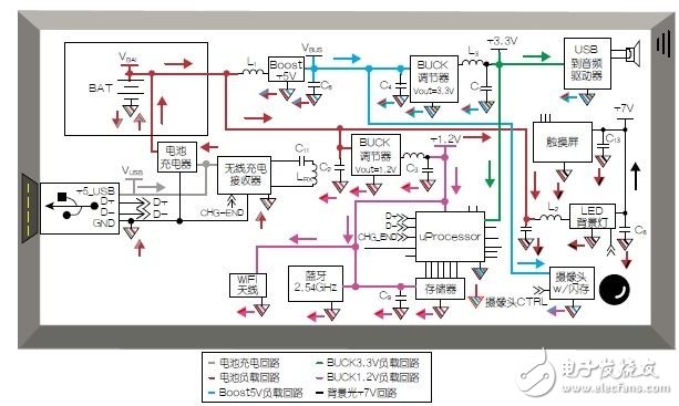
Figure 3: Typical mobile tablet application modules and layout.
Each of the power supplies in Figure 3 is color coded for differentiation, the most important part of which is the GND return current of the color identification. Because multiple power supplies are connected in series, each final load and GND current is forced to complete the return path in the same order as they were powered. For example, the battery powers up the BUCK 1.2V regulator, which powers the microprocessor. Therefore, the current flowing through the microprocessor will return directly to the GND terminal of the BUCK1.2V regulator before returning to the battery. Failure to anticipate the order of completion of all current loops and current paths may result in unstable circuit operation or insufficient GND current return because these issues are not properly considered and controlled in the circuit layout.
It is worth noting that each of the examples listed above assumes a single GND and is drawn on a copper plane that is continuous and uninterrupted in a PCB layer. This ground plane is shared by all the modules in the circuit, rather than separating the GND plane, or separating it into multiple sub-portions, and then using components to connect the GND plane and control the current path. Deliberate module layouts have begun to be implemented because this method uses natural current flow to protect the circuit shield from unwanted GND bounce. Any line carrying current or voltage (positive potential) must have a return path, and the return path should be as close as possible to the positive potential signal and will be distributed to the GND plane below the source/power rail.
After understanding the concept of current flow and minimizing the current loop, a clear conclusion can be drawn that the single-point grounding method is an ideal and preferred method for PCB design because it significantly reduces the number of components, board layers and potential Radiation: Each line and module should have the shortest possible return path on the PCB. In accordance with this guiding principle, system designers only need to control the PCB design from the correct trace width, the intelligent layout of components and modules. He doesn't have to check every line, or build multiple boards to get the right power, signal, and GND schemes. An additional advantage of a single, uninterrupted GND plane layer is that the continuity of the plane allows the generated heat to spread evenly across the entire PCB surface, resulting in lower operating temperatures.
Any signal (or power supply) used to drive any circuit must have an appropriate path back to the source. Circuit designers must consider the source and grounding schemes to properly implement the final system solution. It is critical to consider the load and load type during the implementation phase so that the current paths that cause the voltage bounce are controlled. In areas where GND noise does not affect PCB performance, layout and positioning of those current paths is key to achieving efficient and efficient circuit design.
Gaming headphones, which are suitable for playing games, have extraordinary sound quality - true, clear, and surrounding feeling makes your pulse accelerate and excited.For game users, a high-performance Gaming Headset allows players to experience the immersive feeling in the game. For the gaming players, the gaming headset should also be able to assist the game player to improve combat effectiveness.
Among so many headsets, Gaming Headsets have a sensitivity advantage. The relatively closed listening environment is also more conducive to the game player to feel the details of the sound and improve the judgment of the sound. Therefore, compared with the traditional headphones, the gaming headset has the advantage of positioning ability, and can express the sense of direction of the sound, and is more suitable for expressing the sound clearly in the 3D games. Moreover, the game headsets that serve the player generally also enhance the low-frequency sense, thereby promoting the game plot and making it easier for the player to fully devote himself to the game, thereby achieving "listening to the voice and walking through the hundred steps."

Gaming Headsets
Wireless Gaming Headphones,Bluetooth Gaming Headset,Gaming Headset,Wireless Gaming Headset
Shenzhen Linx Technology Co., Ltd. , https://www.linxheadphone.com