
With the continuous improvement of the level of science and technology, traditional wired communication has become increasingly unable to meet people's needs due to its own limitations, and wireless communication technology has developed rapidly. Nowadays, there are many kinds of wireless communication technologies. Currently, there are WiFi, Bluetooth, UWB, ZigBee, Nordic nRF and TI's SimpliciTI. Different wireless communication technologies have great differences in cost, power consumption, transmission rate, frequency band of use, and functions. It is necessary to select a suitable wireless technology for different needs.
For low-cost, low-power requirements of portable devices, Bluetooth and WiFi consume relatively large power, UWB specifications are not uniform and chip prices are high, Zigbee's transmission rate is limited to only 250 kbit/s, and SimpliciTI is supported by TI's hardware platform. limit. Considering various factors, the system adopts Nordic Semiconductor's 2.4 GHz low-cost and high-performance nRF24L01 radio frequency chip, which is controlled by low-power ARM series STM32L152RD microprocessor to realize short-range wireless data communication. The nRF24L01 not only provides a true ultra-low power solution, but also has excellent coexistence, and its carrier monitoring function ensures reliable communication under WLAN interference. High-speed frequency switching time reduces the possibility of mutual interference with frequency hopping systems such as Bluetooth.
1 hardware designThe design idea of ​​the system is to reduce the power consumption as much as possible while satisfying the high-speed data transmission. Therefore, the balance between performance and power consumption is emphasized in the selection of the MCU and the wireless chip. The hardware part of the system adopts the modular design idea, which is mainly composed of the power supply module, nRF24L01 RF module and microcontroller module. The power supply module has many solutions according to actual needs, and this article does not describe it in detail.
1.1 nRF24L01 RF Module
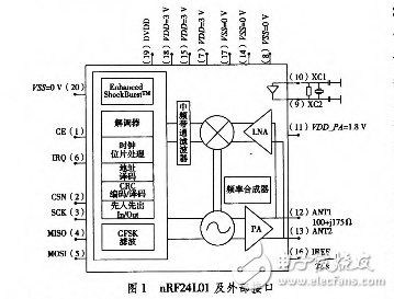
The nRF24L01 is a GF-SK single-chip transceiver chip from Nordic Semiconductor. It operates in the 2.4 to 2.5 GHz world wide (ISM) band and has a transmission rate of 2 Mbit/s. The chip includes a frequency generator, power amplifier, enhanced SchockBurstTM mode controller, crystal and modem. Operating parameters such as transmit power and channel selection can be set via the SPI interface. The enhanced ShockBurstTM feature makes software design simpler and integrates the link layer required for two-way communication, which typically requires a high-speed MCU and large memory space and high power consumption. The nRF24L01 and external interface are shown in Figure 1.
1.2 Microcontroller Module
Based on the high-quality ARM Cortex-M3 core, the STM32L152RD combines high performance with ultra-low power consumption with built-in high-speed memory and operates at 32 MHz. It features an optimized energy-saving architecture and a 0.13μm STMicroelectronics ultra-low leakage production process. In addition, for ultra-low power consumption, the STM32L152RD is also divided into six operating modes to achieve the lowest power in any set time. Consume to complete the task. The STM32 controller's SPI (Serial Peripheral Interface) allows the chip to communicate with external devices in full-duplex or half-duplex, synchronous, serial, and can be used in a variety of applications, including two-wire simplex using a bidirectional data line. For synchronous transmission, reliable communication using CRC check can also be used.
Usually the SPI is connected to external devices through 4 pins. MISO: Master input/slave output pin, which sends data in slave mode, receives data in master mode; MOSI: master output/slave input pin, which sends data in master mode , receiving data in slave mode; SCK: serial port clock, as the output of the master device, input from the device; NSS: slave device selection. This is an optional pin that is used to select the master/slave device.
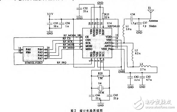
In addition to using the four pins of the MCU to connect to the wireless module, the system also controls the chip select terminal CE of the nRF24L01 through the PA0 pin, and the PB0 pin controls the interrupt response. 2 is a schematic diagram of the interface circuit of the microcontroller module STM32L152RD and nRF24L01.
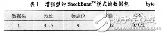
The built-in link layer of the nRF24L01 radio frequency chip makes the software design simpler. The system does not need to configure complex communication protocols for wireless communication. It only needs to program and configure the SPI communication interface between the RF chip and the MCU, and then put the valid data into the transmission. The TX buffer, the chip will combine the address information and the valid data of the TX buffer with the internally generated data header, flag bit and CRC check code to pack and send the data. Table 1 shows the data packets for the enhanced ShockBurstTM mode. The software design part of the whole system is divided into four parts: initialization operation, configuration transmission mode, configuration reception mode, and configuration interruption.
2.1 initialization operation
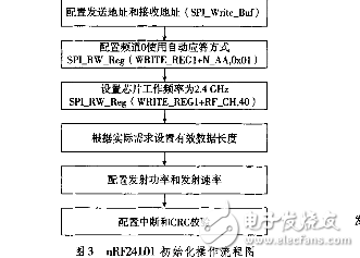
To wirelessly communicate with the radio frequency chip nRF24L01, first initialize the MCU clock, MCU SPI communication port and nRF24L01 [5]. The chip data of the MCU clock and the SPI interface initialization part STM32L152RD are very detailed and will not be described in detail here. The initialization of nRF24L01 mainly includes the configuration of parameters such as address, response mode, working frequency, data length, transmission rate, and interrupt response. The flow chart of the nRF24L01 initialization operation is shown in Figure 3.
2.2 Configuring the send mode
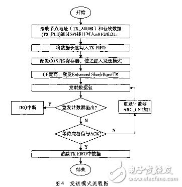
The nRF24L01 is configured for the enhanced ShockBurstTM transmission mode. When the MCU has data to transmit nRF24L01, the Shock-BurstTM mode is started, and the data header, flag bit and CRC check code are automatically generated and transmitted. After the data is transmitted, it will go to the receive mode and wait for the ACK response signal from the receiver. If the ACK response signal is not received, the data is considered to be lost, and the nRF24L01 will cyclically resend the packet until the ACK is received or the number of retransmissions exceeds the value set in the retransmission register. If the number of data retransmissions exceeds the initial set value, a data overflow will result in an IRQ interrupt. When receiving the ACK response signal, nRF24L01 considers that the last packet of data has been successfully transmitted, the data in the TX_FIFO register is cleared and an IRQ interrupt is generated to notify the MCU. The MCU controls the nRF24L01 to enter the transmit mode, receive mode or standby mode according to the task requirements. The sending mode flow is shown in Figure 4.
Configure the send mode code as follows:
Void nRF24L01_TxPacket(unsigned char*tx_buf)
{
NRF24L01_MODE_CE_0 (); SPI_Write_Buf (WRITE_REG1 + RX_ADDR_P0, TX_ADDRESS, TX_ADR_WIDTH); / / write receive address
SPI_Write_Buf (WR_TX_PLOAD, tx_buf, TX_PLOAD_WIDTH); / / write / / data to be sent
SPI_RW_Reg(WRITE_REG1+CONFIG, 0x0e); // IRQ interrupt, 16-bit CRC
NRF24L01_MODE_CE_1();//CE is set to 1, excitation enhanced ShockBurstTM
Send mode
Delay_us(20);//Note that the delay value cannot be too low
}
High Speed Blender,Ipl Laser Hair Removal,Diy Laser Hair Removal,Best Ipl Hair Removal,Epilator Ipl
SHENZHEN CHONDEKUAI TECHNOLOGY CO.LTD , https://www.szfourinone.com