

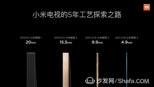
The primary reason is naturally inseparable from the continuous innovation of products. Since the first generation of millet televisions, they have taken a slim line. The first generation of TVs released in 2013 was only 20mm at the thinnest point, 9.9mm to the third generation, and 11.6 in one, with a 65-inch curved TV in the middle, a thinness of only 5.9mm, and a 4.9mm to the millet TV. Millet TV has been Leading TV industry thinness.
Remote control innovation, Xiaomi TV in 2013 with the first TV release of the remote control is only 11 keys, easy to use, and in order to further simplify the operation, the current millet remote control adds a voice keyboard, a key can voice control the TV Most of the features.

System innovation, although the MIUI TV version system is good enough, but millet TV is not satisfied, in September 2016 launched the PatchWall artificial intelligence system to understand the content and understand the user. As of March 2017, this artificial intelligence system upgrades the voice function. With one voice key, keyword search, popularity ranking, open application games, query weather calendar, multiple rounds of dialogue, control of television, and title can be achieved. There are 10 categories of voice interaction functions such as name, star search, movie and television encyclopedia, and intelligent error correction. This completely subverts the interaction of television in the past, and further uses fools.
Sound Quality Innovation: Due to the limitation of the traditional TV, the sound quality of the traditional TV is not satisfactory. So in 2014, Xiaomi TV 2 launched an innovative and independent external sound bar Soundbar and wireless subwoofer. In 2015, Xiaomi TV 3 The industry's first "split design" and upgrading to surround sound in 2016, to the millet TV in 2017, the industry's first Dolby panoramic sound, from Soundbar to Dolby panoramic sound, millet TV led the revolution in TV sound quality, but also attracted The industry has followed suit.
For an Internet TV, only innovation is not enough, there must be strong hardware support. In this respect, Xiaomi TV does not blindly follow the industry. Since the launch of the first generation of TV in 2014, it has adopted the industry's leading quad-core configuration, 2GB of large memory, and 8GB of storage to provide consumers with a smooth experience. Later generations continued the quad-core configuration, and when they went to Xiaomi TV 4A series, they adopted a 64-bit quad-core processor that could support HDR and provided a 32GB version, and then went to the current flagship millet TV 4, 65-inch upgrades. To 3GB large memory, 32GB storage, each generation of product configuration in the industry over the same period, are in a leading position.
Numerous innovations, leading the industry's configuration, and millet TV's quality requirements are also very stringent. In order to ensure the beauty of the products, millet TV engineers have not hesitated to improve the process, and in order to give the user a better picture quality, Wang Chuan broke news about millet. TV has voluntarily destroyed a number of TVs with four-color 4K screens worth more than 7 million, which all show Xiaomi TV's insistence on quality.

Of course, for a popular TV, there must be a price that is close to the people. In this regard, Xiaomi TV has always practiced the concept of “being the best TV in the world and making it affordable for everyoneâ€, so it is based on television products. Cost pricing, I believe we also found that, in the same size with the configuration of television products, millet TV is basically one of the lowest, and from the millet TV 4A series of multiple sizes repeatedly won the market sales championship, which shows the ultra-high millet TV Cost-effective.
Millet TV has been insisting on these, but other Internet TV brands are still buying feelings, difficult innovation, how can we accumulate.
2017 is not over yet. There is reason to believe that Xiaomi TV will rely on those deep accumulations and will further burst out more energy, thus further widening the gap with other Internet TV brands until it is far ahead.
6 Layer PCB
6 Layer PCB - stackup & prototype & price & manufacturing
What is 6 Layer PCB?
6 layer PCB board is, in general, a 4 Layer PCB board with 2 extra signal layers added between the planes. The 6-layer PCB classic stackup includes 4 routing layers (2 outer layers + 2 internal layers) and 2 internal planes (one for ground and the other for power). This enhances the EMI dramatically by offering 2 buried layers for high-speed signals and 2 surface layers for routing low-speed signals. The signal layers should be closed to the adjacent planes.
6 Layer PCB Prototype Fabrication China Manufacturer
Jinghongyi PCB has been committed to the production of multi-layer PCB and prototype PCB for nearly 10 years. The largest number of multi-layer printed circuit boards for customers are 4-layer, 6-layer, 8-layer, 10 layer, 12 Layer PCB and above. In order to ensure the quality of PCB products, we constantly improve and upgrade the production process. PCB surface treatment technology has hot air leveling(HASL), OSP, electroless nickel, immersion gold, immersion silver, immersion tin and so on.
The printed circuit board is basically composed of the pad, via, solder mask layer, silkscreen layer, copper wire, and other parts. Among them, solder mask refers to the part covered by ink on PCB. Because most PCB uses green ink, the green ink part that can be seen is solder mask. The role of the solder mask in controlling the reflow welding process is very important. In addition to green ink, the welding layer can According to the different needs of customers, and can also be customized in a variety of colors, such as green, blue, black, red, white, yellow, purple. Of course, the price will vary with the color of the solder mask. Green oil is the one with low price and stable quality, which is also the reason why green oil is most used. The price of black oil, red oil, and white oil is almost the same, slightly more expensive than green oil, and the price of rare inks such as yellow and violet oil is the highest. In addition to the color of the solder resist ink, there are also matte and bright, matte ink color.
Based on our very experienced PCB engineer, we can help you in the 6-layer PCB stack up and design as much as possible.
In addition to providing you with 6-layer PCB and prototype manufacturing, we also provide one-stop prototype assembly services, including electronic components procurement, stencil, etc. The turnkey printed circuit board assembly services make your R&D work easy and time-saving.
6 Layer PCB Stackup and Design
What is PCB stack UP?
PCB Stack up refers to the arrangement of copper and insulation layers that make up PCB before the layout design of circuit board. Although stacking allows you to get more circuits on a single board through various PCB layers, the structure of PCB stacking design has many other advantages:- The PCB layer stack can help you minimize circuit noise and radiation and reduce impedance and crosstalk problems in high-speed PCB layouts.
- A good stacked PCB stack can also help you balance the need for low-cost, efficient manufacturing methods and focus on signal integrity issues.
- Proper PCB stacking can enhance the electromagnetic compatibility of your design.
- For PCB-based applications, stacked PCB configurations are usually good for you.
Why do PCBs stack up?
The irreversible development of modern electronic products has increasingly pushed PCB towards such needs as miniaturization, light weight, high speed, better functionality and reliability, and longer life, which has led to the popularity of multi-layer PCB. Two or more Single Sided PCB and/or Double Sided PCB are stacked together by a combination of semi-solid adhesives called "prepregs" to form multilayer PCBs through reliable predefined interconnections between them. There are three or more conductive layers in a Multilayer PCB, two of which are outside, and one is synthesized in an insulating board. With the increasing complexity and density of PCB, some problems may arise, such as noise.
One of the most important factors to determine the performance of product electromagnetic compatibility (EMC) is to plan the optimal multi-layer stack up. The carefully designed cascade can minimize radiation and prevent the circuit from being disturbed by external noise sources. Good stacked PCB substrates can also reduce signal crosstalk and impedance mismatch. However, poorer stacking may increase EMI radiation, because impedance mismatch will lead to reflection and ringing in the system, which will greatly reduce the performance and reliability of the product. Then, this article will focus on the layer stack definition, design rules and basic considerations.
Most six-layer PCB consist of four signal routing layers and two planes. From an EMC perspective, a 6-layer Printed circuit board is usually better than a 4 layer PCB board.
6 Layer PCB Stackup

6 layer 1.6 MM standard stackup and thickness

Fig. 1 One of the stackup methods of 6-layer PCB
With six layers available the principle of providing two buried layers for high-speed signals is easily implemented as shown in Fig. 2. This configuration also provides two surface layers for routing low speed signals.

Fig. 2 Less common 6 layer PCB stackup
Not nearly as common, but a good performing stack-up for a six-layer PCB is shown in Fig. 2.

Fig. 3 Another performing six-layer PCB board stackup
Another excellent performing six-layer PCB board stackup is shown in Fig. 4. It provides two buried signal layers and adjacent power and ground planes and satisfies all five objectives. The big disadvantage, however, is that it only has two routing layers -- so it is not often used.

Fig. 4 Another excellent performing six-layer PCB board stackup

6 Layer PCB Stackup for EMI/EMC

EMI/EMC Return Current 6 Layer PCB Issue

EMI/EMC Return Current 6 Layer PCB Solved

Types of 6 PCB stack up-how to choose?
PCB materials and stackup thickness commonly used in multilayer circuit boards.
| 6 Layer Stackup - 0.8mm thickness | ||||||
| layer order | layer name | material type | material description | dielectric constant | thickness | copper weight |
| 1 | top | copper | signal | 0.035mm | 1 oz | |
| 2116 | prepreg | 4.5 | 0.12mm | |||
| 2 | inner 1 | copper | plane | 1 oz | ||
| core | 4.6 | 0.2mm | ||||
| 3 | inner 2 | copper | plane | 1 oz | ||
| 2116 | prepreg | 4.5 | 0.12mm | |||
| 4 | inner 3 | copper | plane | 1 oz | ||
| core | 4.6 | 0.2mm | ||||
| 5 | inner 4 | copper | plane | 1 oz | ||
| 2116 | prepreg | 4.2 | 0.12mm | |||
| 6 | bottom | copper | signal | 0.035mm | 1 oz | |
| Final board thickness: 0.8mm±0.1mm | ||||||
| 6 Layer Stackup - 1.0mm thickness | ||||||
| layer order | layer name | material type | material description | dielectric constant | thickness | copper weight |
| 1 | top | copper | signal | 0.035mm | 1 oz | |
| 2116 | prepreg | 4.5 | 0.12mm | |||
| 2 | inner 1 | copper | plane | 1 oz | ||
| core | 4.6 | 0.3mm | ||||
| 3 | inner 2 | copper | plane | 1 oz | ||
| 2116 | prepreg | 4.5 | 0.12mm | |||
| 4 | inner 3 | copper | plane | 1 oz | ||
| core | 4.6 | 0.3mm | ||||
| 5 | inner 4 | copper | plane | 1 oz | ||
| 2116 | prepreg | 4.2 | 0.12mm | |||
| 6 | bottom | copper | signal | 0.035mm | 1 oz | |
| Final board thickness: 1.0mm±0.1mm | ||||||
| 6 Layer Stackup - 1.6mm thickness (preferred materials) | ||||||
| layer order | layer name | material type | material description | dielectric constant | thickness | copper weight |
| 1 | top | copper | signal | 0.035mm | 1 oz | |
| 2116 | prepreg | 4.5 | 0.12mm | |||
| 2 | inner 1 | copper | plane | 1 oz | ||
| core | 4.6 | 0.6mm | ||||
| 3 | inner 2 | copper | plane | 1 oz | ||
| 2116 | prepreg | 4.5 | 0.12mm | |||
| 4 | inner 3 | copper | plane | 1 oz | ||
| core | 4.6 | 0.6mm | ||||
| 5 | inner 4 | copper | plane | 1 oz | ||
| 2116 | prepreg | 4.2 | 0.12mm | |||
| 6 | bottom | copper | signal | 0.035mm | 1 oz | |
| Final board thickness: 1.6mm±0.1mm | ||||||
| 6 Layer Stackup - 1.6mm thickness (non-preferred materials but possible) | ||||||
| layer order | layer name | material type | material description | dielectric constant | thickness | copper weight |
| 1 | top | copper | signal | 0.035mm | 1 oz | |
| 2116 | prepreg | 4.7 | 0.2mm | |||
| 2 | inner 1 | copper | plane | 1 oz | ||
| core | 4.6 | 0.5mm | ||||
| 3 | inner 2 | copper | plane | 1 oz | ||
| 2116 | prepreg | 4.5 | 0.12mm | |||
| 4 | inner 3 | copper | plane | 1 oz | ||
| core | 4.6 | 0.6mm | ||||
| 5 | inner 4 | copper | plane | 1 oz | ||
| 2116 | prepreg | 4.7 | 0.2mm | |||
| 6 | bottom | copper | signal | 0.035mm | 1 oz | |
| Final board thickness: 1.6mm±0.1mm | ||||||
| 6 Layer Stackup - 2.0mm thickness (preferred materials) | ||||||
| layer order | layer name | material type | material description | dielectric constant | thickness | copper weight |
| 1 | top | copper | signal | 0.035mm | 1 oz | |
| 7630 | prepreg | 4.7 | 0.2mm | |||
| 2 | inner 1 | copper | plane | 1 oz | ||
| core | 4.6 | 0.6mm | ||||
| 3 | inner 2 | copper | plane | 1 oz | ||
| 7630 | prepreg | 4.7 | 0.2mm | |||
| 4 | inner 3 | copper | plane | 1 oz | ||
| core | 4.6 | 0.6mm | ||||
| 5 | inner 4 | copper | plane | 1 oz | ||
| 7630 | prepreg | 4.7 | 0.2mm | |||
| 6 | bottom | copper | signal | 0.035mm | 1 oz | |
| Final board thickness: 2.0mm±0.2mm | ||||||
6
Layer Stackup - 2.0mm thickness (non-preferred materials but possible)
layer order
layer name
material type
material description
dielectric constant
thickness
copper weight
1
top
copper
signal
0.035mm
1 oz
2116+7628
prepreg
4.7+4.7
0.12mm+0.185mm
2
inner 1
copper
plane
1 oz
core
4.6
0.6mm
3
inner 2
copper
plane
1 oz
2116
prepreg
4.7
0.12mm
4
inner 3
copper
plane
1 oz
core
4.6
0.6mm
5
inner 4
copper
plane
1 oz
2116+7628
prepreg
4.7+4.7
0.12mm+0.185mm
6
bottom
copper
signal
0.035mm
1 oz
Final board
thickness: 2.0mm±0.2mm
6 Layer PCB Quote and Price
6 Layer PCB Prototype Price
Of course, at the same time, we also provide sample production services for other PCB products to verify your design as soon as possible.
With regard to delivery, we can provide 24-hour, 72-hour urgent service. No matter where you are in the world.
6 Layer PCB Manufacturing
- Manufacturable PCB Layers
We have abundant experience in manufacturing multi-layer circuit boards, not only in the production process, but also have many years of professional PCB engineers.So if you have multilayer PCB to produce, no matter how many layers, just let us know.
- What size of 6-layer circuit boards can you produce?
According to our PCB manufacturing capability, we have no size limitation.
- PCB Laminate Types
We offer a variety of PCB laminates ranging from FR4 130Tg for lower heating temperatures up to FR4 180Tg for higher temperatures. Also offered are Polyimide, Taconic, Rogers and Nelco material types.
- Manufacturable Thickness of 6-Layer Circuit Board
As with the number of PCB layers we can manufacture, we still have no restrictions on the thickness of the six-layer PCB and can manufacture it.
- PCB Surface Finish Types
We offer various PCB finishes including HASL (Solder), ENIG, Immersion Silver, Immersion Tin, Hard Gold, Entek/OSP, Unclad, Pb Free HASL, Selective Gold and ENEPIG.
Why order 6 layer PCB from JHY PCB?
You will get it after check below advantages.
1. Good quality and price: We are experienced in producing six layer PCB, cost and time can be controlled well. This can help our customer to order good boards in cost-effective price.
2. Short Turnaround Times:
3. No Minimum Quantity: 1 pcs of PCB can be offered.
4. More orders, more discount.
5. Custom PCB Sizes
Printed Circuit Boards,6 Layer PCB,6 Layer PCB Price,6 Layer PCB Prototype
JingHongYi PCB (HK) Co., Limited , https://www.pcbjhy.com