
Abstract: RF2968 is a single-chip Bluetooth transceiver chip, working in the 2400 ~ 2500MHz frequency band, FSK modulation and demodulation; the chip contains RF transmission, RF reception, FSK modulation / demodulation and other circuits, can receive and send digital signals, in line with Bluetooth The radio specification 1.1 requires. The structure, principle, characteristics and application circuit of RF2968 are given in the article.
1 Overview
RF2968 is a monolithic transceiver integrated circuit designed for low-cost Bluetooth applications. The RF frequency range is 2400 ~ 2500MHz, 79 RF channels, 1MHz step, 1MHz data rate, 140 ~ 175kHz frequency deviation, 4dBm output power, and receiving sensitivity. 85dBm, power supply voltage 3V, transmitting current consumption 59mA, receiving current consumption 49mA, sleep mode current consumption 250μA. The chip provides full-featured FSK transceiver functions. The intermediate frequency and demodulation parts do not require filters or discriminators. They have image suppression front-ends, integrated oscillator circuits, and highly programmable synthesis circuits. Automatically calibrated receiving and transmitting IF circuits can optimize the performance of the connection and eliminate artificial changes. RF2968 can be used in systems such as Bluetooth GSM / GPRS / EDGE cellular phones, cordless phones, Bluetooth wireless local area networks, and battery-powered portable devices. 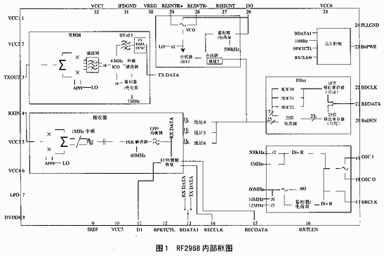
2 pin function
The integrated circuit is packaged in the form of a 32-pin plastic LCC. The functions of each pin are as follows:
VCC1: Supply voltage to the VCO (voltage controlled oscillator) frequency doubling and LO (local oscillator) amplifier circuits.
VCC2: Provides voltage to the RX (receive) mixer, TXPA (transmit power amplifier) ​​and LNA (low noise amplifier) ​​bias circuits.
TXOUT: transmitter output. When the transmitter is working, the output impedance of TXOUT is 50Ω; when the transmitter is not working, TXOUT is in a high-impedance state. Because this pin is DC biased, an external coupling capacitor is required.
RXIN: receiver input. When the receiver is working, 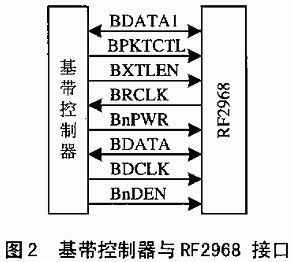 The input impedance of RX IN is low impedance; when the receiver is not working, RXIN is high impedance. An internal series inductor is used in the chip to adjust the input impedance.
VCC3: Provides voltage to the RX input stage (LNA).
VCC4: Provides voltage to the bias circuit of the TX mixer, LO amplifier, LNA, and RX mixer.
LPO: Low-frequency clock output in low-power mode. In sleep mode, this pin can provide a 3.2kHz or 32kHz clock with a 50% duty cycle to the baseband. There is no output in other working modes.
DVDDH: Provides voltage to the RX IF VGA (receiving intermediate frequency voltage gain amplifier) ​​circuit.
IRE F: Connect a precision resistor externally to generate a constant reference current.
VCC5: Provide voltage to the analog intermediate frequency circuit.
D1: This is the charge pump output provided for the clock recovery circuit. Connect an RC network to ground to determine the PLL bandwidth.
BPKTCTL: In transmit mode, this pin is used as a strobe to start the PA stage; in receive mode, the baseband controller can selectively use this pin to signal the detection of the sync word.
BDATA1: Data output from input signal to transmitter / receiver. The input data is unfiltered data at a rate of 1MHz. This pin is bidirectional and is converted to data input or data output according to the transmit and receive modes.
RECCLK: resume clock output.
RECDATA: Resume data output. 
BXTLEN: part of the power control circuit, used to switch on / off the "sleep" mode of the critical chip. After the circuit is powered up from the "OFF" state, when the low-power clock is not working, BR CLK is controlled by the state of BXTLEN (during power-on, BRCLK is first activated by writing BXTLEN and set to high level to enter the idle state) .
BPCLK: Reference clock output. This is the reference clock determined by the crystal oscillator, with a frequency range of 10 to 40 MHz and a typical value of 13 MHz. When the circuit is powered on, BRCLK is activated before the baseband controller sets BXTLEN high. After the circuit enters the idle state, when the low-power clock is not working, BRCLK is controlled by the state of BXTLEN.
OSC O: Same as 19 feet.
OSC I: The OSC pin can generate the reference clock through negative feedback. Connect a parallel crystal and resistor from SOC I to OSC O to provide a feedback channel and determine the resonance frequency. Each OSC pin is connected to a bypass capacitor to provide a suitable crystal load. If you use an external reference frequency, you need to connect to OSC I through a DC blocking capacitor, and connect OSC O and OSC I with a 470kΩ resistor.
BnDEN: Latch the data input to the serial port. Data is latched on the rising edge of BnDEN. 
BDDATA: Serial data channel. Read / write data is sent / output to the shift register on the chip through this pin. The read data is transferred on the rising edge of BDCLK, and the write data is transferred on the falling edge of BDCLK.
BDCLK: The input clock of the serial port. This pin is used to input the clock signal to the serial port. To make the programming time of the hopping frequency the shortest, it is recommended to use the BRCLK frequency of 10 ~ 20MHz.
BnPWR: part of the chip power control circuit, used to control the chip from the "OFF" state to the power-on state.
PLLGND: Ground for RF synthesizer, crystal oscillator and serial port.
VCC6: Power supply terminal of RF synthesizer, crystal oscillator and serial port.
DO: Charge pump output of RF PLL. Connect an RC network to ground to determine the PLL bandwidth. To minimize the setup time and phase noise of the synthesizer, a dual loop bandwidth scheme can be used. At the beginning of frequency detection, a wide loop bandwidth is used. At the end of the detection frequency, RSHUNT is used to switch to a narrow loop bandwidth and provide improved VCO phase noise. The bandwidth conversion time is set by the PLL Del bit.
RSHUNT: By shunting the midpoint of two external series resistors to VREG, the loop filter is converted from narrowband to wideband.
RESNTR-: used to provide DC voltage to the VCO and adjust the center frequency of the VCO. Two inductances are needed between RESNTR- and RESNTR + to form resonance with internal capacitance. When designing a printed board, the inductance from the RESNTR pin to the inductor should be considered. You can add a small capacitor between the RESNTR pin to determine the VCO frequency range.
RESNTR +: See pin 28.
VREG: Voltage regulation output (2.2V). One bypass capacitor is required to connect to ground. Provide bias to the VCO through the loop connected to pins 28 and 29.
IFDGND: Ground terminal of digital intermediate frequency circuit. 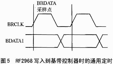
VCC7: digital intermediate frequency circuit power supply voltage.
3 Internal structure
RF2968 is a transceiver designed for Bluetooth applications and working in the 2.4GHz band. Comply with Bluetooth radio specification version 1.1 power level two (+4 dBm) or level three (0 dBm) requirements. For power level 1 (+20 dBm) applications, RF2968 can be used with power amplifiers, such as RF2172. The internal block diagram of RF2968 is shown in Figure 1. The chip contains transmitter, receiver, VCO, clock, data bus, chip control logic and other circuits.
Because the IF filter is integrated in the chip, RF2968 requires only a minimum of external components to avoid external devices such as IF SAW filters and symmetric-asymmetric converters. The high-impedance state of the receiver input and transmitter output can eliminate the external receiver / transmitter switch. The RF2968 is connected to the antenna, RF bandpass filter, and baseband controller to implement a complete Bluetooth solution. In addition to RF signal processing, RF3968 can also complete the baseband control of data modulation, DC compensation, data and clock recovery functions.
The RF2968 transmitter output is internally matched to 50Ω and requires an AC coupling capacitor. The receiver's low-noise amplifier input is internally matched to 50 Ω impedance to the front-end filter. The receiver and transmitter connect a coupling capacitor between TXOUT and RXIN, and share a front-end filter. In addition, the transmit channel can be amplified to +20 dBm by an external amplifier. Turn on the RF2968's transmit gain control and receive signal strength indication to enable Bluetooth to work at power level one. RSSI data is input through the serial port, and provides a resolution of 1 dB when the power range exceeds -20 to 80 dBm. The transmission gain is controlled within 4dB steps and can be set via the serial port.
The baseband data is sent to the transmitter via the BDATA1 pin. The BDATA1 pin is a bidirectional transmission pin, used as an input terminal in the transmission mode, and used as an output terminal in the reception mode. RF2968 implements Gaussian filtering of baseband data, FSK modulated intermediate frequency current controlled crystal oscillator (ICO), and intermediate frequency IF up-conversion to RF channel frequency.
The frequency generated by the on-chip voltage controlled oscillator (VCO) is half of the local oscillator (LO) frequency, and then multiplied to the precise local oscillator frequency. The two external loop inductors between RESNTR + and RESNTR- set the adjustment range of the VCO. The voltage is fed from the on-chip regulator to the VCO. The regulator is connected between the two loop inductors through a filter network. Due to the need for Bluetooth fast frequency hopping, loop filters (connected to DO and RSHUNT) are particularly important, and they determine the VCO's transition and setup time. Therefore, it is highly recommended to use the component values ​​provided in the circuit diagram.
RF2968 can use 10MHz, 11MHz, 12MHz, 13MHz or 20MHz reference clock frequency, and can support 2 times the reference clock of these frequencies. The clock can be sent directly to the OSC1 pin by an external reference clock through a DC blocking capacitor. If there is no external reference clock, you can use a crystal oscillator and 2 capacitors to form a reference oscillation circuit. Whether it is an externally or internally generated reference frequency, use a resistor connected between OSC1 and OSC2 to provide the proper bias. The frequency tolerance of the reference frequency must be 20 & TImes; 10 -6 or better to ensure that the maximum allowable system frequency deviation remains within the demodulation bandwidth of RF2968. The LPO pin uses a 3.2kHz or 32kHz low-power clock to provide a low-frequency clock to the baseband device in sleep mode. Considering the minimum power consumption in sleep mode, and flexibly selecting the reference clock frequency, a 12MHz reference clock can be selected.
The receiver uses a low-IF structure to minimize external components. The RF signal is down-converted to 1MHz so that the IF filter can be embedded in the chip. The demodulated data is output at the BDATA1 pin, and further data processing is completed with baseband PLL data and clock recovery capacitors. D1 is the base pin of the baseband PLL loop filter. The synchronous data and clock are output on the REDATA and RECCLK pins. If the baseband device uses RF2968 for clock recovery, the D1 loop filter can be omitted. 
4 Application
RF2968 radio frequency transceiver as the physical layer (PHY) of the Bluetooth system, supports the Blue RF (Bluetooth Radio Frequency) interface between the physical layer and the baseband device.
There are 2 interfaces between RF2968 and baseband. The serial interface provides channels for controlling data exchange, and the bidirectional interface provides channels for modulation and demodulation, timing and chip power control signals. The interface between the baseband controller and RF2968 is shown in Figure 2.
Control data is exchanged between the RF2968 and the baseband controller through the DBUS serial interface protocol. BDCLK, BDDATA and BnDEN are all signals conforming to the serial interface. The baseband controller is the master control device, which initiates all access operations to the RF2968 register. The RF2968 data register can be programmed or retrieved according to the specific command format and address. The data packet is transmitted MSB first. The format of the serial data packet is listed in Table 1.
Table 1 Serial data packet format
| area | Number of bits | Comment |
| Device address | 3 [A7: A5] | The physical layer is "101" |
| Read / write | 1 [R / W] | "1" for reading, "0" for writing |
| Register address | 5 [A4: A0] | The maximum value of 32 registers |
| data | 16 [D15: D0] | RF2968 is programmed in write mode and returns the contents of the register in read mode |
In the "write" cycle, the baseband controller drives each bit of the data packet on the falling edge of BDCLK. After the data register is set to the high state, RF2968 is updated by the contents of the shift register when the first falling edge of BDCLK arrives, as shown in Figure 3 As shown.
In the read operation, the baseband controller sends the device address, READ bit (R / W = 1) and register address to RF2968, followed by a toggle bit lasting half a clock cycle. This toggle bit allows RF2968 to drive its request signal through BDDATA on the rising edge of BDCLK. After the data bit is transmitted, the baseband controller drives BnDEN to a high level, and re-controls BDDATA when the falling edge of the first BDCLK pulse arrives, as shown in FIG. 4.
The register address field can address 32 registers, and RF2968 only provides register addresses of 3 to 7 and 30 and 31. Different functions can be realized by setting the data of the register.
The two-way interface completes data exchange, timing and state machine control. All bidirectional synchronization (timing) comes from BRCLK, which is generated by RF2968. RF2968 uses the falling edge of BRCLK. Figure 5 shows the general timing when data is transferred from RF2968 to the baseband controller.
The chip control circuit of RF2968 controls the power-down and reset state of other circuits in the chip, and sets the device to the required transmission, reception or power saving mode. The control input of the chip is input from the baseband controller (BNPWR, BXTLEN, BPKTCTL, BDATA1) through the bidirectional interface, and also can be input from the register of the output terminal provided by DBUS (RXEN, TXEN). The baseband controller and the state machine in RF2968 maintain the state of controlling the direction of the bidirectional data line. The baseband controller controls the state machine in RF2968 and ensures that data contention will not occur during reset and normal operation. The commonly used states of RF2968 are:
OFF state-all circuits are powered off and reset, and the setting data is lost.
IDLE state-standby mode. The data is read into the control register, the oscillator remains active, and all other circuits are powered down.
SLEEP state-the chip usually enters this mode from IDLE mode. At this time, all circuits are powered down but not reset, so the data is retained. The circuit can also enter SLEEP mode from other modes, but the TXEN and RXEN states remain unchanged so that the TX and RX circuits remain on.
TX DATA state-data is transmitted in this mode (synthesizer is stable, data channel is synchronized).
RX DATA state-The received data is sent to the baseband circuit via BDATA1 (out of sync) and REDATA (synchronized with RECCLK).
A typical application circuit (GSM telephone) of RF2968 is shown in Figure 6.
Lithium Battery Chargers,48V Lithium Battery Charger,48V Bike Lithium Battery Charger,48V Bicycle Lithium Battery Charger
Changxing Deli Technology Co., Ltd. , https://www.delipowers.com