
Abstract: TS7515 is a high-performance single-chip modem integrated circuit produced by SGS-THOMSON. The chip has superior performance and is convenient and flexible to use. This paper introduces the principle and application of TS7515 single-chip digital modem, and gives the pin function, working principle and typical application circuit of the chip.
1 Introduction
With the development of the network, communication between two computers has become very easy. However, the communication between two computers that are far away must still use a telephone line to reduce costs. At the same time, a modem must be installed on each computer to convert the digital baseband signal to an analog signal that can be transmitted by the telephone line. .
TS7515 is a high-performance single-chip modem produced by US SGS-Thomson Corporation. The chip integrates analog and digital technologies, with low power consumption and low adjacent channel interference. It can work in both the 1200PSP and 600BPS DPSK synchronous mode, and it can also work in 2000BPS And 600KBPS DSK character asynchronous mode (10, 11 bits)? It can also work in FSK mode of 0-300BPS. It also has the ability to automatically monitor dial lines and monitor breakpoint signals. In addition, the TS7515 also has a direct interface with standard microprocessors. The operating temperature range of the TS7515IP is -25 ° C to + 85 ° C.
2 Pin function
Figure 1 shows the pin arrangement of the TS7515 chip in a DIP28 package. The pin functions are as follows:
V +: + 5V power terminal;
V-: -5V power supply terminal;
GND: ground;
XTAL_IN: oscillator input;
XTAL_OUT: oscillator output;
CLK: clock terminal; 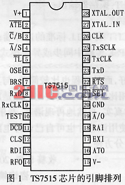
C / B: Selective end of CCITT or BELL standard;
A / S: Selective end of synchronous or asynchronous mode in DPSK transmission;
TL: the selection end of the detection circuit;
OSE: Overspeed selection in asynchronous character mode required by CCITT recommendation;
BRS: It is used to select the corresponding working speed of the chip according to the C / B standard;
CLS: character length selection;
A / O: answering / calling mode selection;
TxD: send data end;
ATO: analog signal output terminal;
EXI: external sound input terminal;
ATE: Answer tone enable terminal;
SEI: scrambling code enable terminal;
TxCLK: Modem's sending clock;
TxSKL: the sending clock of the terminal;
RTS: input terminal for sending request;
RDI: Receive demodulator input;
RAI: analog receiver input;
RFO: the output of the receiving filter;
DCD: data carrier detection end;
RxD: receiving data end;
RxCLK: Receive clock end;
TEST: detection end.
figure 2
3 The internal structure principle of TS7515
The internal structure of TS7515 is shown in Figure 2. The circuit is mainly divided into two modules: transmitter and receiver.
3.1 Launcher
The transmitter section contains 2 analog signal generators that immediately follow the switched capacitor filter. In the phase modulation mode, an optional scrambler in front of the DSPSK modulator can ensure the continuous change of the bitmap transmission, to avoid the loss of the receiving modem when demodulating a continuously repeated data bit (it can also be Disabled during handshake). In the character asynchronous transmission mode, it is mainly used for the conversion from asynchronous to synchronous.
3.2 Receiver
The receiver contains a band-pass filter, an amplifier and a limiter. After filtering, the received signal is amplified and fed into the carrier detector. Because the demodulator used in the TS7515 adopts zero-crossing detection technology, the received signal must be limited before entering the demodulator, and then the output can be detected by the DPSK demodulator or FSK demodulator according to the selected standard. During the call setup or data detection process, the TEST terminal is used to monitor the output of the DPSK demodulator. The DPSK demodulator is followed by a descrambler and an optional synchronous to asynchronous converter, where the descrambler is used to decode the original data. In the working mode of the asynchronous character format, the data buffer can detect the missing stop bit and reinsert it. In addition, the DCD terminal can monitor the level of the received signal. Once the input terminal of the demodulator receives a valid signal suitable for demodulation, the output level of the terminal will be pulled down.
4 Application of TS7515
The application circuit of TS7515 is shown in Figure 3. Since C / B = 0 and BRS = 0, the TS7515 chip works in CCIT V. 22 Standard full-duplex mode, the modulation type is dual symbol DPSK, and the data rate is 1.2 kbps. And because CLS = 1, OSE = 1, A / S = 0, so the circuit works in asynchronous mode, the character length is 10 bits.
image 3
When the circuit is working, the computer sets the TS7515 to answer / calling mode through the control line and interface line of the microprocessor EF6801, and then performs internal scrambling to transfer the data to be sent to the TxD terminal, and passes through the asynchronous to synchronous converter inside the chip , Scrambler, DPSK modulator generates analog modulation signal, and then through the transmission filter with equalization scheme to the ATO end (analog signal output)? Finally through D. A. A (direct access circuit) is transmitted to the telephone line.
The received DSPSK modulated signal is also passed through D. A. A is transmitted to the RAI terminal (analog signal input terminal), then internally filtered and equalized, and output to the RFO terminal (receive filter output terminal), and then coupled to the RDI terminal (receiver demodulator input terminal) through a 1μF capacitor. To meet the level detection conditions. Then recover the baseband data through the internal DSPSK demodulation circuit, and the baseband data is then decoded, descrambled, and synchronized to the asynchronous converter, and finally the demodulated data is serially output at the RxD end (receiving data end) and passed through the micro The interface line of the processor is passed back to the computer.
In order to optimize the working performance of the TS7515, special attention should be paid to the decoupling of the power supply and wiring diagram wiring. The power supplied to the digital system may contain large spikes and other noises. In order to eliminate noise, the power supply should be bypassed with tantalum capacitors and electrolytic capacitors. These capacitors should be close to the TS7515 chip. In order to improve the high-frequency characteristics, ceramic capacitors should be bypassed next to the electrolytic capacitors. The power cable should be as short and straight as possible. And try to avoid ground loops. The wiring should minimize the coupling between the analog input and the digital line. The RDI end (13 feet) is particularly sensitive to noise. The connection of this terminal through ceramic capacitor and RFO (14 feet) terminal should be as short as possible. In short, through careful layout, the coupling of the connection with the digital signal should be avoided as much as possible to avoid power supply noise and common ground noise to ensure the effective operation of the chip.
Bldc Motor,48V Bldc Motor,Bldc Motor 24V,57 Series Bldc Motor
Jinan Keya Electron Science And Technology Co., Ltd. , https://www.keyaservo.com