
1 Introduction
In actual operation, if the main controller of the inverter is dead or reset, the inverter will stop output and stop the load motor, which will cause huge losses to the power plant. For the most widely used cascaded multilevel inverters, this paper uses the inverter inertia output technology based on fpga, that is, when fpga detects the abnormality of the main controller, it maintains the output of the inverter according to the memory value until the controller returns to normal. Will greatly improve the stability and reliability of the inverter.
2 Cascaded multi-level inverter works
Cascaded multi-level inverters, also known as unit series multi-level inverters or perfect harmonic-free inverters, achieve high-voltage output by connecting several low-voltage power units in series, with low harmonic content of voltage and current, and harmonic pollution to the power grid. Smaller, the input power factor is higher, and it is not necessary to use the input harmonic filter and power factor converter, which is widely used in practice [1]. Taking 6kv inverter as an example, each phase consists of 6 power units with rated voltage of 577v in series. There are 18 power units in three phases, which are respectively powered by 18 secondary windings of the input isolation transformer, and 18 secondary windings are divided into 3 groups. There is a phase difference of 20° between each group, which is equivalent to 18-pulse rectification. The total distortion rate is only 3%, and the total current distortion rate is less than 4%. Its structure is shown in Figure 1.
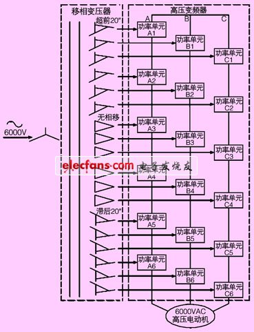
Figure 1 Cascade 6kv inverter structure diagram
The structure of the power unit is shown in Figure 2. After three-phase AC rectification, the DC bus voltage is formed by filtering capacitors. The inverter consists of four igbt modules with a withstand voltage of 1700v. The h-bridge single-phase inverter circuit is controlled by pwm. At the output end, the AC output of the variable voltage frequency conversion is obtained, and the output voltage is single-phase AC 0-577v, and the frequency is 0-50hz. The bypass function is a function that causes the device to continue to operate normally after the device has failed. When bypass is required, the thyristor v is turned on, bypassing the power unit output, and when normally operating normally, the thyristor v is in an off state.

Figure 2 Cascade inverter power unit structure
3 phase shift carrier spwm modulation method based on fpga
The basic principle of phase shift carrier technology is to generate spwm signals using several 1.2khz triangular carrier signals and a sinusoidal reference signal (per phase). Appropriate phase shifting of the triangular carrier eliminates a certain number of harmonics. Taking phase a as an example, the sinusoidal modulation wave and the triangular carrier are as shown in Fig. 3. The amplitude and phase of the sinusoidal modulated wave used in the six-stage power unit are the same, and the triangular carrier shape of each power unit has the same phase, and the phase angle between the carriers is sequentially shifted by 2π/6 or 60°, so that the output voltage can be effectively suppressed. And current rate of change. The modulated wave phases of the left and right bridge arms of the h-bridge unit are opposite in phase, which helps to increase the equivalent carrier ratio of the entire system. Tests have shown that the equivalent carrier frequency when n-level cells are connected in series is 2n times the frequency of the triangular carrier, and the DC voltage utilization under the control of this mode is high.
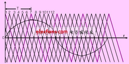
Figure 3 Phase shift carrier modulation schematic
At present, the inverter used generally puts the above comparison process in the cpu. When the cpu encounters interference reset or program error, the inverter will stop output. The comparison process of triangle wave and sine wave by fpga will solve this problem well. The cpu's powerful computing power can be used to calculate the sine wave participating in the comparison in real time. The fpga high-speed clock can be used to accurately generate the phase-shifted triangle wave, and then in fpga. Compare the output.
The Samsung S8 Plus Battery replacement have been undergo thoroughly tested,we have stricter QC inspection standards than other regular suppliers.All Samsung phone batteries built-in certified Grade A+ battery cells,CE,FCC and RoHS certified.Our Samsung S8 Plus battery replacement will provide you with up to 500 lifetime charge cycles,work as good as your original Galaxy S8 plus battery.
As a professional manufacturer over 7 years experience,we Hequanqingnuo technology owns the brand of HQQNUO involved in different kinds of Cell Phone Battery such as Iphone Battery , Huawei Battery , Samsung Battery and other Cell Phone Accessories such as iPhone Charger Case, QI Car Charger ,Wireless Phone Charger etc.

Samsung S8 Plus Battery
Samsung S8 Plus Battery,Battery For Samsung S8 Plus,Samsung Galaxy S8 Plus Battery,Battery For Samsung Galaxy S8 Plus
Shenzhen Hequanqingnuo Electronic Technology Co., Ltd. , https://www.hqqnbattery.com