
Abstract: Aiming at the solution of TV format PAL / NTSC signal output VGA display format, the design and implementation of FPGA-based video format conversion system is described in detail. Using Cyclone III series EP3C1*84C6 as the core processing device, it realizes NTSC/PAL video decoding, color space conversion (CSC), frame rate conversion and interlaced progressive conversion, scaling, video DAC conversion, and finally realizes component R, G, B VGA video format video output, resolution up to 1 600 × 1 200@ 100 Hz.
This article refers to the address: http://
1 system design
The design uses ALTERA's EP3C1*84C6 model FPGA as the video processing core, connecting two DDR2 SDRAMs. The DDR2 chip model is M icron's MT47H 32M16BN _37E. As the system's data storage device, the bandwidth is 32 bit and the clock rate is 200MHz. The rate is 400 Mbps. The video decoder chip is TVP5147, and the video DAC uses high performance ADV7123. The entire system framework is shown in Figure 1.
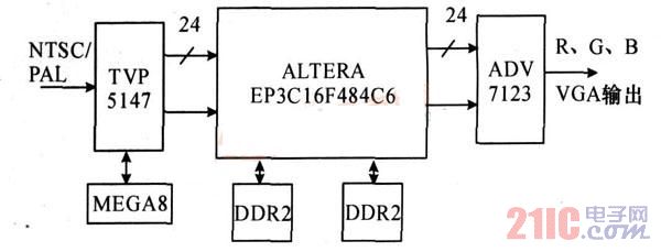
Figure 1 video processing board block diagram
2 hardware function module.
2. 1 video decoding
The decoding process of TVP5147 is shown in Figure 2.
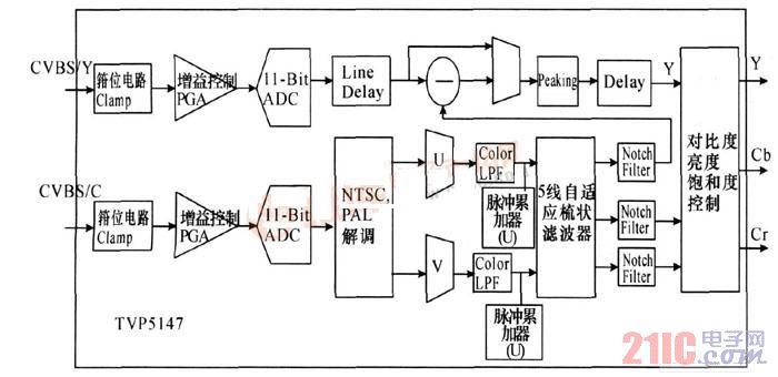
Figure 2 TVP5147 decoding process
After the video decoder chip TVP5147 is reset, the I2C register is properly configured to it through the MCU. The values ​​of the I2C register configuration of the TVP5147 in this paper are shown in Table 1.
Table 1 I2C register settings for TVP5147
2. 2 video memory
A large number of video data memory modules are included in the video processing module, and can be mainly classified into a line memory, a frame memory, and a look-up table memory.
(1) Line memory is used to store data in one line of video. Because the amount of data is not large, it is realized by FPGA internal RAM.
(2) The frame memory is used to store one frame of video data, and is realized by DDR2 due to the large amount of data.
(3) The lookup table memory is used to generate irregular input and output correspondences, such as the Sin function and the gamma correction curve.
2. 3 FPGA Module Design
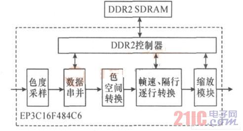
The FPGA module design is shown in Figure 3.
Figure 3 FPGA module block diagram
2. 3. 1 data string and conversion and chroma resampling module
This module is divided into two parts: serial-to-parallel conversion and chroma resampling.
The serial-to-parallel conversion is mainly to convert the mixed data output by the TVP5147 into component data. Due to the BT.656 10-b it 4:2:2 mode, the output data clock is twice the pixel clock ( 13. 5 MHz), and the output data is Cb0, Y0, C r0, Y1, Cb1, Y2. , C r1 , etc., this module converts it into 4:2:2 Y'CbCr component data, and the RTL simulation result is shown in Figure 4.
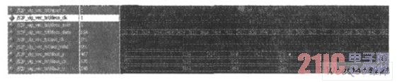
Figure 4 serial and parallel conversion module simulation results
Although video component transmission brings better image reproduction, it also brings about an increase in data bandwidth. Therefore, people often resample the visually less important color difference signals to 4:2:2 ( Or 4:1:1) to reduce the transmission data bandwidth. The 4:4:4 signal is basically used inside the video and display system, so chroma resampling has become an indispensable module in video conversion. This article implements a 4:2:2 to 4%4%4 and 4:4:4 to 4:2:2 conversion. The conversion methods of 4:2:2 to 4:4:4 include direct repetition method, one-dimensional filtering method and brightness adaptive filtering method.
Considering the hardware cost and processing quality, we choose the one-dimensional filtering method, that is, only consider the filtering of the chroma channel in the horizontal direction. Figure 5 is a block diagram of a block for chroma resampling using an n-tap FIR filter.
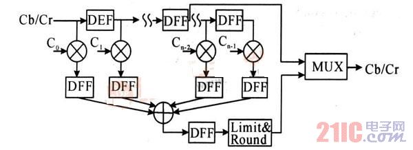
Figure 5 4: 2:2 to 4:4:4 chroma resampling module
2. 3. 2 color space conversion module (CSC)
Since different video standards use different color spaces, and some video processing needs to be processed in a specific color space, color space conversion is necessary. The color space conversion is actually a three-input linear matrix transform to obtain a new three-output. The basic conversion formula is as follows:

Ax, Bx, Cx, and Sx in the above equation represent conversion coefficients between different spaces, respectively. The color spaces involved in a typical video system include the R'G'B' space of a computer, the Y'UV space of NTSC and PAL, and the Y'CbCr space. FIG. 6 is a block diagram of a conversion module in which conversion coefficients can be arbitrarily configured, that is, the standard is not limited. The 10 b it Y'CrCb in the previous section can be converted to 8 b it BT. 709 standard Y'CrC data by this color space converter using the SD to HD conversion factor.
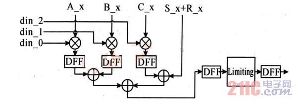
Figure 6 color space conversion module (Rx is round ing value)
Input 8 bit R'G' B' signal, first convert from R' G' B' to Y'CbC r to 10 b it Y' CbC r signal, then convert to 8 bit R' G'B ' signal. The color space conversion adopts the high-definition standard, and the fixed-point fraction of 16 b it is used to process the conversion coefficient. The upper part of the figure is the 8-bit R'G'B' data input, the middle is the 10' it's Y'CrCb data, and the lower part is the 8b it's R'G'B' data output. Due to the pipeline processing, the output has a delay of 3 clocks.
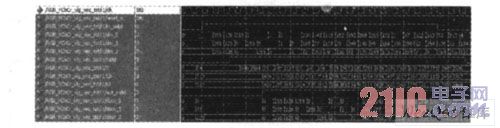
Figure 7 8 b its R'G'B' to 10 bits Y' CbC r and then back to 8 b its R'G'B' simulation results
2. 3. 3 frame rate conversion and interlaced progressive conversion module
The method of interlaced to progressive can be divided into two aspects: airspace and time domain. The spatial domain algorithm is simple and easy to implement in hardware. It is common to have direct repeat rows and rows that are missing in the vertical direction. The time domain method involves operations between adjacent fields. Common methods include field mixing, motion adaptive deinterlacing, and the most complex motion compensation deinterlacing algorithm. This paper compromises the use of the field mixing method, which combines the adjacent fields of the field data into progressive frame data, as shown in Figure 8.
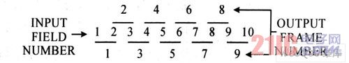
Figure 8 Field mixing method to achieve interlaced progressive transformation
The field frequency of the PAL and SECAM systems is 50 Hz, while the NTSC is 60 Hz. Field frequency conversion is required when superimposing different field frequency signals. Most video devices use a frame rate of 60 Hz, so this article only covers frame rate conversions of 50 to 60 Hz. Common methods include field repetition, field interpolation, and motion compensation. The field interpolation algorithm is shown in Figure 9.
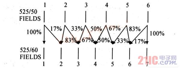
Figure 9 Field interpolation method from 50 Hz to 60 Hz
As for the PAL system, as can be seen from the above two figures, as long as the three rows of data can be read simultaneously, the interlaced progressive conversion and the frame rate conversion can be completed once. If the first frame of the output is determined by the first and second fields of the input data, the second frame of the output is determined by the first, second, and third fields of the input data, and the third frame of the output is the second and third of the input. 4 field data decisions, and so on.
The system uses a DDR2 memory with a bit width of 48 as the field memory, while the data width at the DDR2 controller side of the FPGA is 96. If the output of the second frame is generated, when the first field is stored, the upper 64 bits are masked and not written, and the lower 32 b is written to the field data (actually only 30 b it is used). When the second field is stored, the upper 32 bits and the lower 32 b it are masked and not written, and the middle 32 bits are written to the field data. When the third field is stored, the low 64 b it is masked and not written, and the high 32 bit is written to the field data. In this way, when the data is read, three fields of data can be read simultaneously, and then the combined interpolation operation described above can be performed to obtain an output. The format of the field memory data is as shown in FIG.
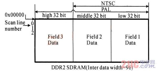
Figure 10 Field memory that enables simultaneous deinterlacing and frame rate conversion
Note that the new input field data cannot cover the adjacent data, so the mask bit is constantly beating when the data is stored, and the period is 5 fields. Although this reduces the efficiency of writing, since all data reading and writing are sequential operations, the access efficiency of DDR2 is still improved as a whole, and the operation is simplified. For the NTSC system, since the frame rate conversion section can be ignored, it is possible to store only two fields using the lower 64-bit portion.
2. 3. 4 zoom module
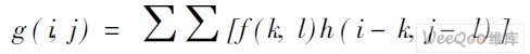
Video scaling includes both up scaling and downsca ling, and the basic method of scaling is spatial interpolation. The following equation is a general mathematical expression for interpolating an image, where g ( i, j) is the pixel value of the point to be interpolated in the scaled image, and f ( k, l) is the pixel at the coordinates ( k, l) in the original image. The value, h( i- k,j - l) is the interpolation basis function.
There are many choices of interpolation basis functions, usually two-dimensional rectangular functions, linear functions, cubic functions and S inc functions, which correspond to nearest neighbor interpolation, linear interpolation, cubic interpolation and ideal interpolation (actually using S The inc function is truncated and interpolated. The interpolation effect is from poor to good, but the difficulty of implementation is also improved. In the actual processing, the interpolation is used to implement the interpolation basis function, and due to the symmetry of these interpolations, it can be decomposed into two parts, horizontal and vertical interpolation, such as two-dimensional linear interpolation function corresponding to bilinear interpolation (Bilinear Interpo) Lating), the cubic function corresponds to Bicubic Interpolation, and the Sinc interpolation function is actually Po ly phase Interpolation. In this paper, multi-phase interpolation is used to achieve image scaling. In fact, multi-phase interpolation and cubic interpolation are almost the same in the 4 4 ​​domain size, except that the corresponding interpolation function values ​​are slightly different. The multi-phase interpolation method generates an output point by performing phase shift interpolation of the Lanczos2 function on the field corresponding to the original image. As shown in Figure 11.
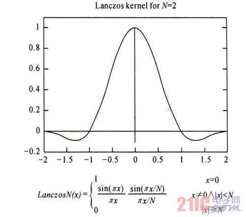
Figure 11 Lanczos2 function
Suppose g ( u,v ) is a point in the scaled output image, which is restored to the nearest point of the original image as f ( i,j) and the coordinates of the difference ( x,y ) between the two are output, then the output point g The mathematical expression of (u, v) is as follows, from which it can be seen that the vertical filtering and the horizontal filtering are actually performed separately in two steps.
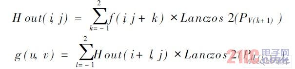
There is a relationship: i = ( u ×W in ) /W out,j = ( v ×H in) /H out; x = ( u × W in)% W out,y = ( v ×H in)% H out. W in and Wout are the image widths before and after scaling, respectively, and Hin and H out are the image heights before and after scaling, respectively. Figure 12 shows the horizontal vertical phase of the 4 × 4 field, where the horizontal phase values ​​are PH 0, PH 1, PH 2, and PH 3, and the vertical phase values ​​are PV0, PV1, PV2, and PV3, respectively. Multiphase filtering can be achieved by obtaining 8 phase values ​​from the x, y values ​​obtained from the above relationship.
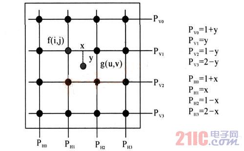
Figure 12 4 × 4 field horizontal vertical phase
Figure 13 is a block diagram of the filter part of the image scaler designed in this paper. The vertical horizontal lookup table stores the values ​​of Lanczos2 function of four different phases.
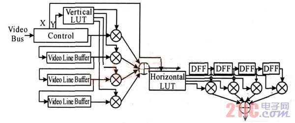
Figure 13 Filter in the image scaler
2. 4 video DAC
The video is encoded into analog R, G, and B. The video DAC chip ADV7123 has three independent channels and 10 bit high speed DACs, as shown in Figure 14 for its function diagram and its system function.
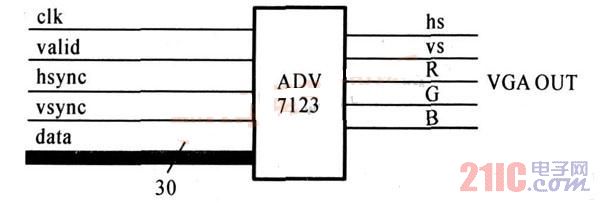
Figure 14 ADV7123 system diagram
3 system power supply design
The reliability of the power supply is the key to the success of the electronic system design. In the case of the design of the power supply, the power supply circuit is required to be considered in consideration of the efficiency of the power supply circuit. The system requires 0. 9 V, 1. 2 V, 1. 8 V, 2. 5 V, 3. 3 V, 5 V A total of 6 power supplies.
The LM2737 has an output current of up to 5 A and an efficiency of up to 90%. The package is SO IC and is small. The VTT of VDDR and VRef of 0.9 V are converted from the DDR reference terminal voltage general-purpose chip TPS51100.
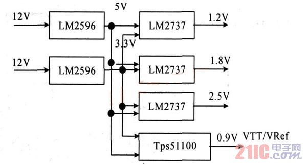
Figure 15 power supply design block diagram
4 Conclusion
In this paper, the video format conversion system is designed by using the EP3C1*84C6 device of C y l lone III and related video codec chip, which realizes the conversion of ordinary TV signal to the more common VGA interface signal, and increases the processing by scaling the video signal. Video resolution. In addition, the use of FPGA as the core video processing device makes the system support for video system with great flexibility.
Silver Zinc Battery For Aircraft
Ag Zn Battery,Ag-Zn Battery For Aircraft,Ag-Zn 45Ah Battery,Silver Zinc Battery For Aircraft
Henan Xintaihang Power Source Co.,Ltd , http://www.taihangbattery.com