

Embedded computing with heterogeneous architectures is fast becoming a reality. Today, we have indeed seen many leading IP and semiconductor vendors developing heterogeneous hardware. In this article, we will illustrate a typical use case for heterogeneous operations and the challenges of moving toward a heterogeneous programming model.
Executing computer vision algorithms with heterogeneous architecture
Figure 1 shows how to use multiple heterogeneous hardware and software components to build a video recording application that supports beautification. In this example, the input frame captured by the ISP/camera is first viewed by the GPU to determine the position of the face and its individual features (such as eyes, lips, nose, and other), and then transfer the coordinates. To the CPU, and the role of the CPU is to track and automatically adjust the focus and exposure of the camera in order to achieve high quality video results.
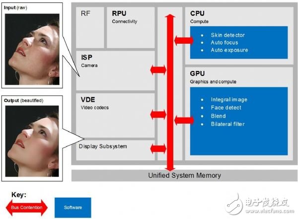
Figure 1: Using multiple heterogeneous hardware and software components to build a video recording application that supports the beautification function.
The CPU can also be used to determine where the skin is on the face, and then the GPU uses a bilinear filter to smooth out the texture and remove artifacts such as spots and wrinkles while preserving facial contours. Sharpness.
The converted image sequence is output to both the hardware encoder and the display subsystem. The former is used to record to the hard disk, while the latter is rendered in the preview window. For additional optimization, the CPU instructs the hardware encoder to encode multiple coordinates of the face with higher fidelity than the background, which simultaneously optimizes video quality and file size. In this case, at least five different hardware components need to access the image data in the memory.
Memory bandwidth limit
An important feature of many SoCs is a single unified system memory, such as DDR DRAM external to the chip, which is shared by all hardware components. These components typically communicate with other components and memories using a shared bus or interconnect architecture, and the bandwidth of the bus and interconnect architecture is typically very limited due to the built-in area and cost.
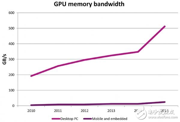
Figure 2: The memory bandwidth of a mobile embedded SoC is much lower than that of a desktop computer.
Compared to desktop-class devices equipped with PCI Express busses, SoCs typically have 10 times less bandwidth, which is a common performance bottleneck - both hardware components want to access both memory and other I/ This is especially true in the case of O.
In addition, when the application passes ownership of the data between different hardware components, the underlying operating system generates duplicate copies of the data in memory. In some cases, this may be due to hardware limitations. For example, the GPU must access the data that the CPU is configured in virtual memory, which is the space that the CPU can arbitrarily page in the hard disk.
In other cases, this may be related to the image format; for example, ISP generates image sensor data in YUV format, but the CPU or GPU needs to filter this data in the RGB color space.
Conversely, some operating systems, like Android, can automatically convert images from YUV format to RGB format (eg OGLES_TEXTURE_2D texture) before providing the data to the developer; for many visual algorithms that only need to process image brightness data, This will reduce their efficiency. When high-resolution imagery is processed at video rates, the inefficiencies caused by these behind-the-scenes data replicas become more severe.
To solve these problems and assist developers in developing high-performance, low-power heterogeneous computing applications, ImaginaTIon has published an image architecture for SoC designers, OEMs and developers. The features discussed in this article are fully supported in the OpenCL driver, and many OpenLone drivers are already built into the mobile platform.
ImaginaTIon's PowerVR imaging architecture enables developers to take advantage of sophisticated image manipulation to create new user experiences, from intelligent vision systems to augmented reality applications and virtual character creation. Designers can use their creativity to create endless possibilities. The only limitation is the processing power of the phone!
Semiconductor Disc Devices(Capsule Type) is the abbreviation of thyristor, also known as Silicon Controlled Rectifier, formerly referred to as thyristor; thyristor is PNPN four-layer semiconductor structure, it has three poles: anode, cathode and control pole; thyristor has silicon rectifier The characteristics of the parts can work under high voltage and high current conditions, and their working processes can be controlled and widely used in electronic circuits such as controlled rectifiers, AC voltage regulators, contactless electronic switches, inverters, and inverters.")
Semiconductor Disc Devices(Capsule Type)
Semiconductor Disc Devices,Inverter Thyristor,Phase Control Thyristor,Capsule Type Semiconductor Disc Devices
YANGZHOU POSITIONING TECH CO., LTD. , https://www.yzpst.com