
BCNet-S7PPI is used for Siemens S7-200 Ethernet programming download, data monitoring, and supports S7-200 SMART, Yiwei, Hexin and other PLCs.
BCNet-S7PPI straight-through type: BCNet extended DSUB9 pin female port, can be connected to Siemens touch screen (Siemens text TD200/TD400, TP/OP), multi-master cable, communication board;
BCNet-S7PPI bridging type: BCNet extended DSUB9 pin female port, can be connected to non-Siemens touch screen, such as Kunlun Tongzhou, Weilun, Delta, Buco and so on.

Features:
1, support multi-master communication, does not occupy the communication port, the expansion port can be connected to the touch screen or other main station.
2. The baud rate is adaptive.
3. Automatically query the address of the master station and display the address list.
4. Installed directly on the PPI communication port of the PLC, no external power supply is required.
5. Support Siemens S7 Ethernet communication driver, including MicroWIN, WinCC and SIMATIC NET.
6. Users can use high-level language programming (such as VB, VC, C#, etc.) according to BCNetS7 protocol to realize data communication with S7-200 and facilitate the development of production management system.
7. Free BCNetS7 OPC server.
8, BCNetS7 DX function, through a simple configuration can be exchanged between the two PLCs.
9, integrated ModbusTCP server, support FC1, FC2, FC3, FC4, FC5, FC6, FC16, Modbus data area is automatically mapped to the S7-200 data area.
10. Support 24 Ethernet TCP/IP connections, allowing 24 PCs to simultaneously collect PLC data.
11. In conjunction with the R-Net 3G/4G series, remote maintenance and data monitoring of the device can be realized.
Typical applications: network port programming download, superior monitoring, device networking. The BCNet expansion port does not occupy the communication port of the S7-200, and can be connected to a Siemens touch screen or a non-Siemens touch screen.
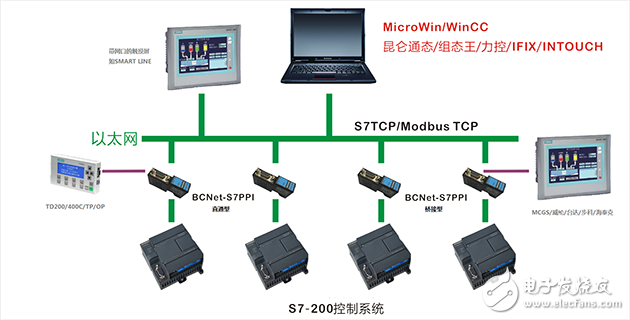
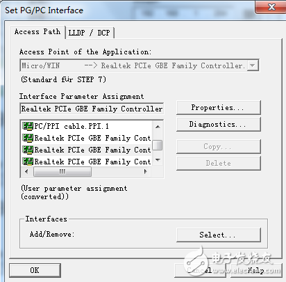
Application (1) : Supports Siemens Ethernet driver. When MicroWIN connects to S7-200, it is similar to CP243-1. S7-200 does not need to be configured.

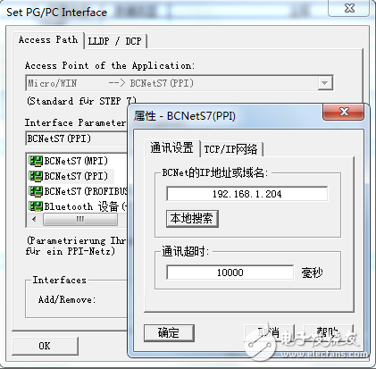
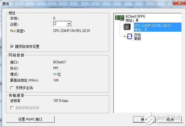
Application (2) : Support BCNetS7 (PPI) driver.
Application (3): Free BCNetS7 OPC server, no connection limit and number of points, support SOCKET programming, easy to develop production management system.
Example (1): WinCC is directly connected to the S7-200 via a TCP/IP channel.
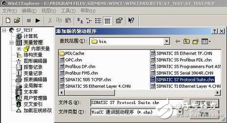
(1) Open the WINCC software, create a new project, right click "Variable Management", select "Add New Driver" and select "SIMATIC S7 Protocol Suite.chn".
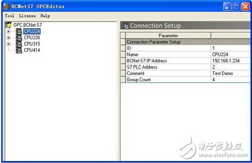
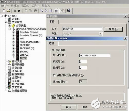
(2) Right-click the "TCP/IP" connection, select "New Driver Connection", define a connection name, click "Properties", fill in the IP address of BCNet-S7PPI at "IP Address", click "OK" .
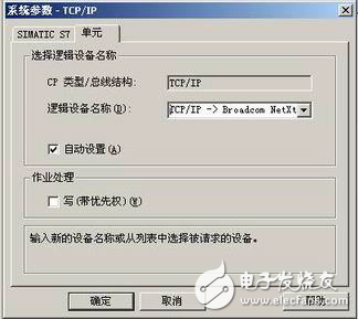
(3) Right-click the "TCP/IP" connection, select "System Parameters", and select "TCP/IP->Your Network Card" in the "Logical Device Name (D)" in the "Unit" option.
Example (2): It can be used as a ModbusTCP server for S7-200 and S7-200 SMART, allowing Modbus TCP client access.

More products: BCNet-S7MPI, BCNet-FX, BCNet-Q, BCNet-CP, BCNet-CJ.
Via in Pad PCB
What is Via in Pad? In shortly,via in pad is the via holes are at the SMD pad.The vias are very small,usually under 0.3mm.Why and how? First is there is no enough space to layout,you have to put the vias and holes closer even together.Second it helps thermal management and for high frequency boards,it may help improve signals.
Because the SMD pads are for SMD components loading,so the solder can not flow to inner layer or the other side when assemble.That is the most important for via in pad board.
How PCB manufacturers like us to do via in pad board? We will fill all vias with non-conductive epoxy and plate copper over it ,so the vias are flat same as others. Many PCB factories are unable to do such capability.
The key technology is how we fill vias and guarantee there is no any solder (surface finishing) in the holes.
Filled via in pad is a way to achieve intermediate density with an intermediate cost compared to using blind/buried vias. Some of the key advantages associated with using the via in pad technology are:
.Fan out fine pitch (less than .75mm) BGAs
.Meets closely packed placement requirements
.Better thermal management
.Overcomes high speed design issues and constraints i.e. low inductance
.No via plugging is required at component locations
.Provides a flat, coplanar surface for component attachment
Via in big pads are not a big problem.but for BGA,that is technology.As BGA pads are very small,10mil or 12mil,and there is no enough space.Manufacturing is not easy as other boards.
Via In Pad PCB,6Layer Via In Pad PCB,Touch Pad PCB,Via In Pad
Storm Circuit Technology Ltd , https://www.stormpcb.com