
One: How does the PSR architecture achieve constant current output on the secondary side?
Before PSR, the constant current control that I can imagine is to connect a resistor in series with the line that wants to monitor the current level, and realize the feedback by checking the voltage signal at both ends of the resistor to achieve the current level control, or at least one CT (current detection transformer) monitors the current flowing through it. It may be that affluence limits my imagination. I can't think of the two detection elements mentioned above on the secondary side of PSR, you can't find it even with a magnifying glass! So the magic thing is coming, how is the secondary side current constant control realized? Don't worry, first present the PSR ECG-key working waveform chart 1:
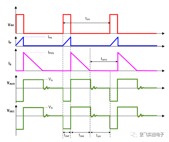
figure 1
The above figure Is is the secondary inductor current waveform, which is a triangular ramp, then its average current ILAV=1/2Is, which is half of the triangle waveform waist, but this is not the load current Io. Because of this inductor current The discharge time in a complete cycle tw is only the time of tons, so the average value of the entire cycle is the value of the output current Io: Io=1/2Ipks*tons/tsw (1). Because the control chip is on the primary side , So we think this needs something to do with the original side. We know that the secondary side current Ipks and the primary side current Ipk are inversely proportional to the primary side turns ratio Nps, that is, Ipks=Ipk*Nps(2). Combining formulas (1) and (2) can get: Io=1/2Ipk *Nps*tons/tsw (3). Observing formula (3), it can be found that the peak current Ipk of the primary side can be controlled according to the CS PIN threshold of the chip (when the voltage on Rcs reaches the internal Vsc_ref threshold of the chip, Q1 is turned off, and the maximum value of VCS_ref is a fixed constant : 500mV) (Figure 2), and the tons conduction time is the period from the time when the primary side Q1 is turned off to the end of the falling edge detected by FB, and then the chip deliberately increases or decreases the primary and secondary sides without conducting The dead time toff (Figure 1) adjusts the operating frequency tw, so that tons/tsw is fixed at 1/2, and the primary and secondary turns ratio Nps is fixed with the determination of the transformer, so the chip controls Ipk and tons/tsw The size of Io finally controls the size of Io (Io=1/4*Ipk*Nps), so that the control of Io is completed without any detection resistance on the secondary side, and constant current is realized. At the same time, because the primary side FB completes the tons calculation by detecting the falling edge, it can only work in DCM or BCM. And here the charger is only 5V/2A specifications, and the current peak value of working in DCM will not be too large. At the same time, TSW is constantly changing, so the system works in PFM mode.
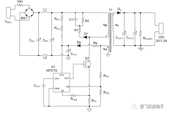
figure 2
2. Transformer design steps:
Transformer parameters include inductance Lp, primary secondary turns ratio Nps, primary secondary turns Np and Ns, etc. The online calculation formulas for such parameters are dazzling and seem to be easy to calculate. However, the author believes that with different topologies, the method and sequence of determining the above parameters will change as the control strategy of the chip is different. Taking this case as an example, without considering the stress of the primary and secondary sides, it is hoped that the larger the turns ratio Nps, the better, so that the current on the primary side can be minimized when the maximum output current has been determined, and the heat will be generated during low-voltage operation. Also the lowest. Some chips also have a QR mode. The larger the turns ratio, the greater the voltage Vor that Vo refracts to the primary side, and the lower the trough that falls during resonance. This helps reduce turn-on loss and ultimately improves efficiency. But can Nps keep improving? What is the ceiling that restricts its elevation? (First eliminate the stress, after all, we can choose a power device with higher withstand voltage). This has to return to the conclusion of the constant current control in the previous chapter, the system must not work in CCM mode. So under what circumstances can the system easily enter the CCM mode? Here is a conclusion: when the system works at the lowest input voltage and outputs the maximum current load, it is the closest to the CCM mode. The proof is as follows: No matter how the system works, the volt-second balance of the primary and secondary sides must always be observed, so it is obtained: Vin_dc*Dp*tsw=Vs*Nps*tons (4) where Vin_dc is the DC voltage on the bus capacitor, Dp is the duty cycle when the primary side is on (yes, I still introduced the concept of duty cycle in the PFM control), Vs is the voltage across the secondary side inductor, which is the output voltage Vo plus the rectifier diode The conduction voltage drop Vf is obtained. I don’t need to introduce other familiar parameters. The specific definition is shown in Figure 1. Derived from the formula (4): Dp=Vs*Nps*tons/(Vin_dc*tsw) (5). Observing formula (5), you will find that when other parameters are fixed, Dp is proportional to Nps, that is, the larger the turns ratio Nps, the larger the duty cycle Dp of the primary side conduction, then Dp can always increase ? First look: tsw=tonp+tons+toff (6) As the load continues to increase, the toff time is continuously reduced (see Figure 3), so that tSW will continue to decrease and the operating frequency will become higher and higher until toff drops to 0. At this time, tsw=tonp+tons (7). We know that for a fixed output of a fixed system, the secondary side degaussing time tons is also fixed (tons=Ipks*Ls/Vs), and the chip will let the parameter tons/tsw The bottom line of 0.5 is firmly held, so as the load increases, tonp can "swallow" the part of toff, but not the part of tons, so the maximum tonp/tsw can only reach 0.5, that is, the maximum Dp is 0.5 .At this time, the system is working in the BCM state (critical conduction), which is also the upper limit of the power that the system can give to the secondary side. At this time, if the voltage on the bus capacitor drops a little bit, see formula (5), Dp is required Further increase, but the maximum Dp can only reach 0.5, and it can be concluded from formula (5) that Vs must also drop, that is, the output voltage will also drop significantly. We know that when the input low voltage is fully loaded, the voltage on the bus capacitor presents a McDonald's steamed bun wave shape (you can look at its logo if you haven't eaten McDonald's). The waveform has peaks and valleys, and the valley corresponds to Vin_dc_min. When the valley voltage is so low that the required Dp is greater than 0.5, because the chip cannot respond to the "non-divided" requirement, it eventually leads to a periodic drop in the system output voltage, which is the source of power frequency ripple. . .
After analyzing so much, it can be concluded that after Nps increases to a certain value, the problem of power frequency ripple cannot occur at low voltage and full load, that is, Vin_dc_min coincides with the maximum duty cycle of 0.5 on the upper primary side. Formula (4) derives Nps≦(Vin_dc_min*Dp*tsw)/(Vs*tons)=Vin_dc_min/Vs *0.5*2 (8) to get the maximum value of Nps.
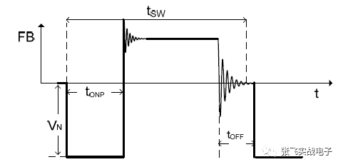
image 3
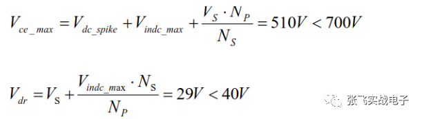
The voltage stress of the primary and secondary side can be calculated as follows:
Voltage stress of primary side switch tube: Vce_max=Vdc_spike+Vindc_max+Vs*Nps (9)
Stress of the secondary side rectifier tube: Vdr=Vindc_max/Nps+Vs (10)
The above Vdc_spike is the voltage spike caused by the leakage inductance, which can be suppressed by the primary snubber, and the recommended value is 120V. According to the above formula, the primary side MOS and the secondary side diode can be selected.
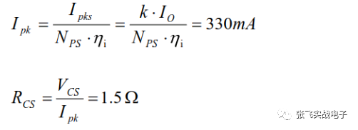
The next thing to be determined is the primary side peak current Ipk, which is obtained by formula (3) Ipk=4Io/Nps (11)
After IPk is determined, because the internal CS pin reference voltage Vcs_ref of the chip is 0.5V, once the voltage on the sampling resistor RCS reaches 0.5V, the switch is turned off and tonp ends. Rcs=Vcs_ref/Ipk(12). Rcs needs to be taken from the actual resistance series and fine-tuned according to the actual situation. Considering the sampling accuracy, the accuracy of Rcs is recommended to be 1% or less.
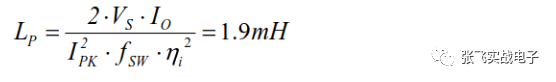
Next, we need to determine the transformer inductance. In some applications, the inductance is determined by the current ripple rate r, but in this case the system has been working in DCM, so r is a fixed value: 2. Therefore, we cannot use this formula to determine the magnitude of the inductance Lp. Since there is no restriction of r, naturally I want to make the sense of Lp smaller, so that the size of the transformer can be smaller and smaller, so can we reduce the size of Lp as we want? At this time, we should naturally think of this formula: Po=1/2Lp*Ipk ²*fsw*η (13) where Po is the system output power, Lp is the primary side inductance, Ipk is the primary side peak current, and fsw is the work Frequency, η is efficiency. It can be seen that if the output power does not change and Ipk is already a fixed value, fsw will gradually rise as Lp decreases. So what are the rising ceilings of fsw? First of all, this case uses a triode drive. The operating frequency of the triode cannot be too high due to the recovery of the stored charge. It is recommended to be below 60KHZ. At the same time, the chip FB voltage sampling has a fixed delay such as 4.2us. This delay is to avoid the ring generated when the primary side Q1 is just turned off to prevent sampling distortion. If the working frequency continues to increase, but the sampling delay is fixed, then the tons has ended after 4.2us, which will also cause sampling distortion. Here fsw is recommended to be 60KHZ, so that Lp=2Po/( Ipk ²*fsw*η) (14)
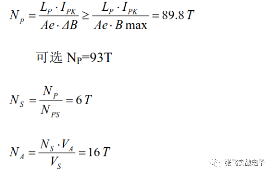
The following needs to determine the number of primary and secondary turns: the value of primary turns should ensure that the magnetic is not saturated, that is, Np≧(Lp*Ipk)/Ae*Bmax. Among them, Ae is the effective core area of ​​the selected transformer, and Bmax is The maximum flux change is recommended for general ferrite materials such as PC40 as 0.3T. After both Nps and Np are determined, the number of secondary turns Ns=Np/Nps; and the number of auxiliary winding turns Na=Ns*Va/ Vs, where Va is the voltage of the auxiliary coil, the recommended value is about 11V. Why this value is used? This involves a large change in the voltage on the VCC capacitor of the flyback circuit at no load and full load.
First of all, because the energy pulse is very weak and the interval time is long when there is no load or light load, the transformer can be equivalent to an inductance. After the primary side Q1 is turned off, this primary inductance injects energy into the secondary side and the auxiliary winding side. For the primary winding, it is indistinguishable between the secondary side and the auxiliary winding side. These two windings are equivalent to loads, which means that the secondary side and the auxiliary side grab energy (this is like food shortages). Everyone is rushing to eat), so you will observe that the voltage on the primary side Vcc capacitor Cvcc fluctuates greatly, and it may fall from 11V to 9V, and the chip VCC has a UVLO under-voltage protection point. Once the protection is triggered , The chip protection restarts. . . . Therefore, we hope that when the VCC voltage is higher at light load, this undervoltage protection point will not be triggered.
However, the VCC voltage cannot be too high, because when the load is full, the energy pulse is larger than the no-load, and the pulse frequency is very high. At this time, the energy is sufficient, and the voltage fluctuation on the VCC capacitor is very small. It's not like robbing each other for energy like during light load (this is like food is rich, everyone is full but humility to each other, I want each other to eat more, don't hold on). At the same time, there is another uninvited guest to the VCC capacitor at full load, that is, the RING generated when the primary side is just turned off. This RING is also energy, which will be coupled to the auxiliary winding side and finally transferred to the VCC capacitor, making the VCC voltage rise very high. It does not satisfy the formula of the turns ratio with the secondary side voltage. If the VCC voltage rises to 27V, the VCC overvoltage protection will be triggered, and then you will find a strange phenomenon. After adding full load, the machine keeps restarting. You thought it was overload protection, but it actually triggered VCC overvoltage. Protected. This is why the VCC voltage should not be too high at light load. What if it is really high? The slow recovery of the VCC winding rectifier diode can help digest and absorb a part of the energy brought by the RING to help the VCC voltage decrease. Or increase the resistance of Ra appropriately (Figure 2).
Well, the parameters of the transformer are determined through the above steps: Nps, LP, Np, Ns. We can find that the method and order of the above parameters are determined to a certain degree. There are many formulas for calculating transformers on the Internet, but they cannot be used casually. They should be determined according to the actual chip control strategy and working mode. This is a bit like a game-playing solution. Fan part. In the next chapter, we will cite actual cases to analyze the parameter determination process step by step, and strive to make everyone feel more specific. At the same time, we will explain clearly the principles of input high and low voltage line compensation and output line compensation.
High and low voltage current compensation design
The following explains the design of input high and low voltage cross flow point balance. First of all, we have to understand why the constant current point is different when input high voltage such as 264V and input low voltage 90V? This involves the concept of the edge (slope) and threshold of the analog circuit, as shown in Figure 1. When the voltage generated by the primary current peak value on the primary sampling resistor reaches t1 of the threshold voltage Vcs_ref set inside the chip, the chip plans to Turning off the switching tube, but affected by the delay of the chip itself and the switching tube, the real turn-off time is at t2, and the corresponding voltage is Vcs_ref', which causes the actual current peak value to be larger than the expected setting of the chip ( In order to demonstrate, it has been appropriately exaggerated), and the slope of the current rise on the primary inductor under high voltage is greater than that at low voltage. After the same delay tdelay=t2-t1, the error Vcs_ref' will be greater. As a result, the output current will be larger when high-voltage input is compared with low-voltage input. This extra â–³VCS=Vcs_ref'-Vcs_ref=(Vin_dc/Lp) *tdelay*RCS is the object we want to eliminate, which can be seen by the formula If it is directly proportional to the DC component of the input voltage, can we introduce another parameter to make it also proportional to Vin_dc, but in the opposite direction to achieve the purpose of offsetting â–³VCS? With this idea, we can build a suitable circuit, and my chip AP3772 contains this circuit, as shown in Figure 2:
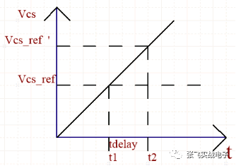
figure 1
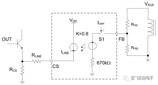
figure 2
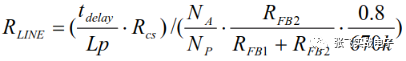
When the primary side switch tube is turned on, the bus voltage on the BULK capacitor will be coupled to the Vaux auxiliary winding through the winding and detected by the FB pin. At this time, S1 has been closed and a current flows through Rline. The voltage Vcs_line is used to compensate, then you can adjust the resistance of Rline to set the compensation voltage. The formula is as follows:
The negative voltage Vn of the FB pin is linearly related to the line voltage:
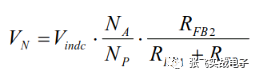
The compensation voltage Vcs_line is,
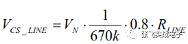
This voltage compensates for the increase â–³VCS caused by the delay of the chip and the switch tube on the primary inductor current, so Rline can be obtained to achieve accurate output current under different line voltages.
Of course, if the chip does not have this kind of compensation, you can also connect a resistor divider on the bus voltage to Rline to achieve compensation. The idea is the same, but compared to the one with built-in compensation, not only the number of BOMs Will increase, and standby power consumption will also increase.
Output cable cable compensation design
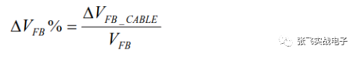
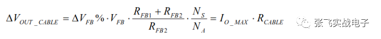
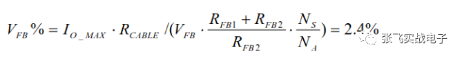
Since the charging cable is relatively long and has a certain resistance, a certain voltage drop will inevitably occur after the current passes. At the same time, the voltage drop is linearly related to the magnitude of the current. Our chip is to meet the linear compensation of the voltage drop of different output cables under different applications. On demand, there are three versions of the chip to choose from. Inside the chip, an increment â–³VFB_cable is superimposed on the VFB to superimpose a corresponding increment â–³Vout_cable on the output voltage Vout, and this increment is linearly related to the output current. The AP3772 barrel detects the output load current through the CPC pin and then transmits a linearly related increment to the VFB to achieve cable compensation.
A related parameter â–³VFB_cable/VFB% is specifically defined on Datashet (Figure 3). For example, in AP3772, this value is 6%, which means that the increment of VFB superimposed on full load is 6%, and if the output When the current is 10% of the full load, then this increment is 0.6%, which is completely linearly related to the size of the current. This and the line loss cancel each other out, which just makes the voltage at the end of the line unchanged. The appropriate chip version can be selected according to the impedance value of the output cable for different applications.
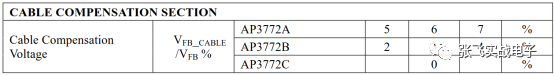
image 3
Hypothesis
Then,
Then
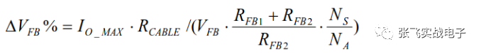
After calculating â–³VFB%, the appropriate chip version can be selected based on this.
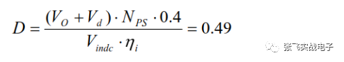
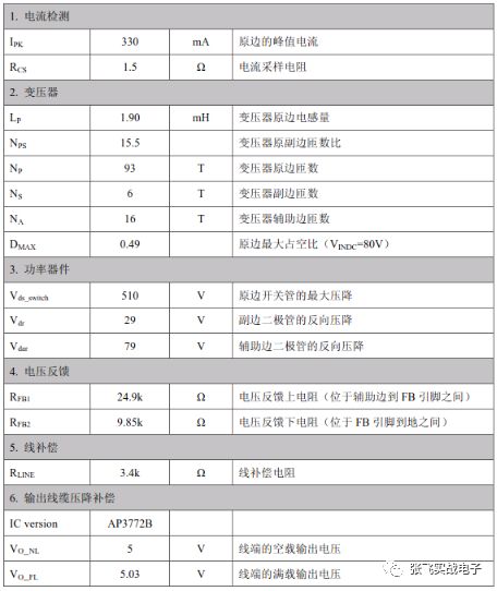
Design example (5V/1.2A system)
Now let's implement the ideas and formulas explained above through the following examples, so that everyone can understand more specifically:
specification:
Input voltage: 85Vac-265Vac
Output voltage at the cable end: Vo_cable=5V
Output full load current: Io=1.2A
Board output voltage: Vo=5.13V, (AWG22 cable, length=100cm)
Switching frequency: fsw=65KHZ
Secondary diode conduction voltage drop: Vd=0.4V
Auxiliary diode conduction voltage drop: Vda=1.1V
Vcc voltage: Vcc=14V
Core model: RM5 (Ae=23.7mm²), Bmax
Vdc_spike≦50V (with snubber circuit)
Design steps:
1) Calculate the primary and secondary turns ratio of the transformer (Nps)
Nps≦(Vin_dc_min*Dp*tsw)/(Vs*tons)=Vin_dc_min/Vs *0.5*2=15.5
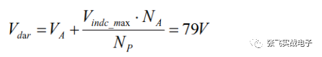
2) Check the maximum voltage stress of the primary side switch tube and the response voltage drop of the auxiliary side diode
3) Calculate the peak current and current sampling resistance of the primary side (Ipk and Rcs)
4) Calculate the primary inductance of the transformer (LP)
5) Calculate the number of turns of the primary and secondary sides of the transformer (Np, Ns, Na)
6) Check the maximum duty cycle of the primary side
7) Detect the response voltage drop of the auxiliary side diode
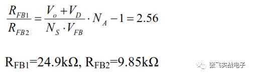
8) Voltage feedback resistance
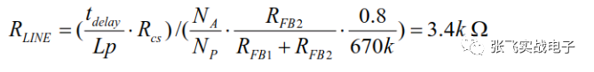
9) High and low voltage current compensation resistor
10) Output cable voltage drop compensation
The VFB of the three versions of AP3772 are 4.04V. Then,
According to the datasheet, AP3772B (3%) version is the best choice.

Here, the output voltage Vo_NL=5V when there is no load, the output voltage on the cable when it is full is slightly higher than when it is no load.
Summary of design results:
Summary
PSR is based on the design of AP3772. The most critical elements include standby power design, switching frequency design, transformer design, voltage feedback resistance design, high and low voltage current compensation resistance and output cable voltage drop compensation design. This chapter gives a design framework based on ideal models and ideal waveforms. Some parameters need to be adjusted appropriately according to specific circuits and application environments.
Incremental encoders provide speed, direction and relative position feedback by generating a stream of binary pulses proportional to the rotation of a motor or driven shaft. Lander offers both optical and magnetic incremental encoders in 4 mounting options: shafted with coupling, hollow-shaft, hub-shaft or bearingless. Single channel incremental encoders can measure speed which dual channel or quadrature encoders (AB) can interpret direction based on the phase relationship between the 2 channels. Indexed quadrature encoders (ABZ) are also available for homing location are startup.
Incremental Encoder,6Mm Solid Shaft Encoder,Hollow Rotary Encoder,Elevator Door Encoder
Jilin Lander Intelligent Technology Co., Ltd , https://www.jilinlandermotor.com