
I. Introduction
As one of the main switching power devices, MOSFETs are widely used in module power supplies. Understanding the loss composition of the MOSFET and analyzing it will help optimize the MOSFET loss and increase the power of the module power supply. However, reducing the loss of the MOSFET and other losses will cause more serious EMI problems, resulting in the system not working stably. . Therefore, it is necessary to reduce the MOSFET performance while reducing the EMI performance of the module power supply.
Second, the power consumption analysis of the switching transistor MOSFET
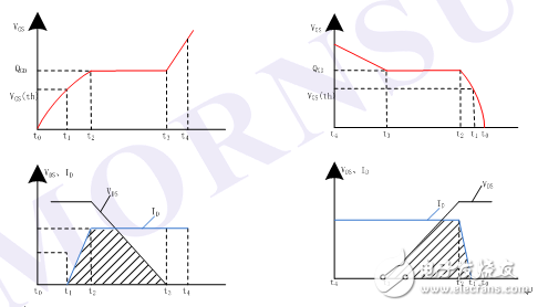
Figure 1. MOSFET turn-off-on waveform conversion. Figure 2. MOSFET turn-on-off waveform conversion.
The loss of the MOSFET mainly consists of the following components: 1. on-state loss; 2. conduction loss; 3. turn-off loss; 4. drive loss; 5. absorption loss; as the module power supply decreases, the switching frequency needs to be Further improvement leads to an increase in turn-on loss and turn-off loss. For example, at a drive frequency of 300 kHz, the ratio of turn-on loss and turn-off loss is already a major part of the total loss.
Losses are generated during the turn-on and turn-off of the MOSFET. During these two conversions, the relationship between drain voltage and drain current, gate-source voltage and charge is shown in Figure 1 and Figure 2. The conversion process is analyzed as an example:
In the interval t0-t1: the gate voltage rises from 0 to the threshold voltage Uth, the switching transistor is turned on, and no drain current passes through this interval without generating loss;
In the interval t1-t2: the gate voltage reaches Vth, the drain current ID begins to increase, and reaches the maximum value at time t2, but the drain-source voltage remains unchanged at the high level. As can be seen from Figure 1, this part has VDS and The IDs overlap and the MOSFET power consumption increases.
T2-t3 interval: From the time t2, the drain-source voltage VDS starts to drop, causing the Miller capacitance effect, so that the gate voltage can not rise and the platform appears. The charge amount is equal to Qgd at t2-t3, and the drain voltage starts to decrease at time t3. Minimum value; this part has VDS and ID overlap, MOSFET power consumption increases
T3-t4 interval: the gate voltage rises from the platform to the final driving voltage (module power supply is generally set to 12V), the rising gate voltage further reduces the on-resistance, and the MOSFET enters a fully-on state; Through loss.
The turn-off process is similar to the turn-on process, except that the waveform is reversed. There are many references for the analysis of the conduction loss and turn-off loss of the MOSFET. The summary formula of the MOSFET Analysis of Zhang Xingzhu is directly quoted here:
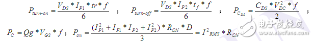
Remarks: For rise time, for switching frequency, for falling time, for gate charge, for gate drive voltage for MOSFET body diode loss.
Third, MOSFET loss optimization method and its advantages and disadvantages
3-1. Reduce MOSFET losses by reducing the drive frequency of the module power supply
From the loss analysis of the MOSFET, it can be seen that the higher the driving frequency of the switching power supply, the higher the conduction loss, the turn-off loss and the driving loss, but the high frequency can make the transformer core of the module power supply smaller and the module volume. It becomes smaller, so the switching frequency can be used to optimize turn-on loss, turn-off loss, and drive loss, but high frequency can cause serious EMI problems. Jinshengyang DC/DC R3 products adopt frequency hopping control method to reduce the driving loss by reducing the switching frequency of the module power supply under light load conditions, thereby further improving the efficiency under light load conditions, making the system more energy-efficient in standby operation. , further improve the working time of the battery power supply system, and also reduce the radiation problem of EMI;
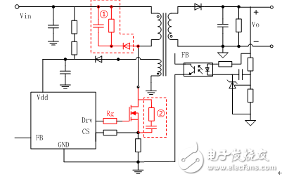
Figure 3. General block diagram of flyback switching power supply
3-2. Reduce MOSFET losses by reducing
The typical low-power module power supply (less than 50W) mostly uses the circuit topology as a flyback. The typical control circuit is shown in Figure 3. The loss analysis from the MOSFET can also be known: proportional to the turn-on loss, and turn-off loss. It is proportional; therefore, it can reduce the loss of MOSFET by reducing. Generally, the driving resistance Rg of MOSFET can be reduced to reduce the time, but this optimization method brings serious EMI problem; the product of Jinshengyang URB2405YMD-6WR3 is To illustrate this problem:
1) The URB2405YMD-6WR3 uses a 10Ω MOSFET drive resistor. The bare metal radiation test results are as follows:
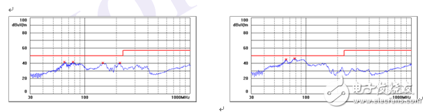
Figure 4 Radiation disturbance horizontal polarization direction test results Figure 5 Radiation disturbance vertical polarization direction test results
2) URB2405YMD-6WR3 uses 0Ω drive resistance, bare metal radiation test results are as follows:

Figure 6 Radiation disturbance horizontal polarization direction test results Figure 7 Radiation disturbance vertical polarization direction test results
From the results of two different driving resistance tests, although the CLASS A level of the radiated disturbance degree of EN55022 can be passed, but the driving resistance of 0 ohm is used, the margin of the test result in the horizontal polarization direction is less than 3 dB. The design of the scheme cannot be passed.
3-3. Reduce losses by reducing absorption circuit losses
In the design process of the module power supply, the leakage inductance of the transformer is always present. In the flyback topology, the MOSFET's drain often has a large voltage spike during the MOSFET turn-off process. In general, the MOSFET The voltage design margin is sufficient to withstand. In order to improve the overall power efficiency, some power supply manufacturers do not increase the absorption circuit (the absorption circuit is labeled as 1RCD absorption circuit and 2RC absorption circuit as shown in Figure 3) to absorb the peak voltage. However, not paying attention to the design of these absorbing circuits is often the main reason for the EMI design failure. Take the absorption circuit of Jinshengyang URF2405P-6WR3 (using the 2RC absorption circuit in Figure 3) as an example:
1) The drive resistance Rg is 27Ω, no RC absorption circuit, and the radiation disturbance test results are as follows:
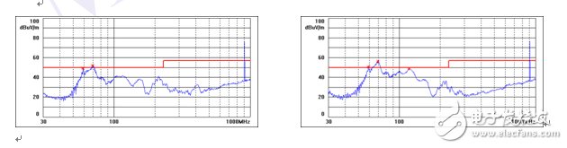
Figure 8 Radiation disturbance horizontal polarization direction test results Figure 9 Radiation disturbance vertical polarization direction test results
2) The drive resistance is 27Ω; the absorption circuit is the resistance R and C 5.1Ω 470pF, and the radiation disturbance test results are as follows:
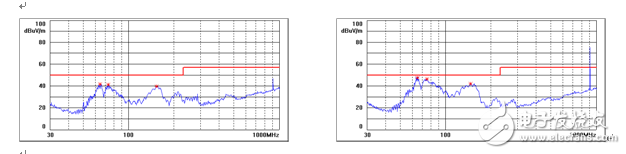
Figure 10 Radiation disturbance horizontal polarization direction test results Figure 11 Radiation disturbance vertical polarization direction test results
From the test results of two different absorption circuit schemes, the scheme of not using the absorption circuit is not able to pass the CLASS A level of the radiated disturbance degree of EN55022, and the absorption circuit can solve the problem that the radiation disturbance degree experiment fails. Different RC combinations can further reduce radiated disturbances.
Fourth, summary
The power optimization of the MOSFET is actually a system engineering, and some optimization schemes even affect the EMI characteristics. In the above case, Jinshengyang R3 series products have deepened the concept of energy saving and environmental protection into the development process of power supply, and well balanced the overall efficiency and EMI characteristics of the power supply, thus further optimizing the power supply parameters. The power parameters are further optimized to be more compatible with the customer's system, and to play the role of a true "heart" of the electronic system, continuously delivering energy.
Road Light,Double Arms Road Light,Off Road Lights,Round Road Light
Yangzhou Heli Photoelectric Co., Ltd. , https://www.heli-eee.com