
introduction
The NioslI embedded processor is a SOPC solution proposed by A1tera. It is a 32-bit embedded processor that can be freely configured and built by users. It can quickly and flexibly build a powerful SOPC system with rich peripherals. Altera offers a number of common IP cores that allow users to easily integrate their own dedicated functions; however, for some specific peripherals, there are no ready-to-use IP cores, such as the LCD module CBGl28064.
Users can add custom IP cores to the SOPC design through custom logic. In practical applications, LCD liquid crystal displays have been widely used in smart instruments, meters and low-power electronic products due to their low power consumption, small size, light weight and simple control drive. Taking the liquid crystal display module CBGl28064 of Shenzhen Akita Vision Industrial Co., Ltd. as an example, the LCD display driver IP core is designed in the SOPC system based on NioslI, and downloaded into the Cyclone series FPGA to realize the display driver for LCD.
1 CBGl28064 liquid crystal display module
CBG128064 is a liquid crystal module with two HD61202 as column drivers and one HD61203 as row driver. The HD61202 is a graphic liquid crystal display controller with a drive output that can be directly connected to an 8-bit microprocessor. The HD61203 can generate line drive signals and various synchronization signals simply by supplying power. The CBGl28064 liquid crystal display module has a built-in display memory RAM, and the display state of each pixel on the display screen is in one-to-one correspondence with each bit data in the display memory RAM. The data of the display memory is directly used as a driving signal for the graphic display. The external processor only needs to set the desired display mode through its 8-bit data line and 6 control lines. Other functions are automatically completed by the module. The HD61202 provides seven simple instructions: display on/off instructions, display start line (ROW) setting instructions, page (RAGE) setting instructions, column address (Y Address) setting instructions, read status instructions, write data instructions, read data. instruction.
2 program selection
There are usually two ways to implement the display driver for the LCD by the Nios II embedded processor:
One is to use off-the-shelf parallel input/output (PIO) cores. The core provides a memory mapping interface from the controller port to the general I/O port of the Avalon bus, connecting the interface of the LCD module to the parallel port of the Nios II embedded processor, and the operation of the port by the Nios II embedded processor. To complete the control of the LCD module. This method is similar to single-chip operation, and the timing is simple and easy to implement. However, in the SOPC system, the hardware needs to design the I/O port connected to the peripheral. The software needs to write the interface program for reading and writing control, which increases the processor time. Overhead, the parallel processing power of the FPGA has not been realized.
The other is to use a custom IP core. Think of the LCD module as an external memory or I/O device. As a slave device attached to the Nios II embedded processor's Avalon bus, the processor controls it by accessing the I/O device or reading and writing memory. This method requires writing the HDL module and defining the control, status, data registers and control bits by itself, which enables flexible timing control. Once the design is complete, it can be packaged as a separate component available for SOPC BLdldel, which can be used like any other peripheral provided by Altera and available to other designers. This article uses this method to achieve.
3 LCD display driver design
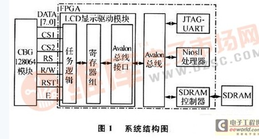
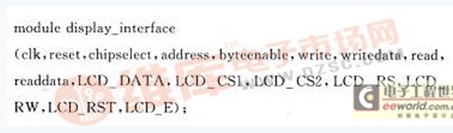
Figure 1 is a system structure diagram. The focus of the design is on the design of the LCD display driver module. According to the modular and hierarchical design idea, the display driver can be divided into three parts, namely the task logic part, the register group part and the Avalon bus interface part. The logic part of the task describes the read/write logic function of the liquid crystal module; the register file part provides the channel for internal register access; the Avalon bus interface part operates the register through the top-level interface module to realize access and control of the behavior module. Among them, DATA[70] is an 8-bit data line, CS1 and CS2 are chip select signals, RS is an instruction/data selection signal, R/W is a read/write selection signal, RST is a reset signal, and E is a read/write enable signal.
3.1 Task Logic
Task logic is the core part of the entire driver. To achieve display control of the LCD, it is necessary to design according to the specifications and timing requirements of the CBG128064 drive controller. In the sequential logic circuit, the cooperation of the data signal and the control signal is more complicated, but it is very important. The finite state machine can be used to design a complicated digital circuit system.
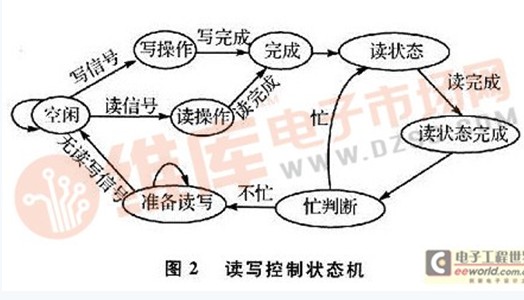
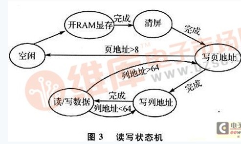
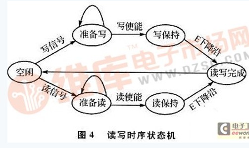
This paper uses a finite state machine to implement the core logic of the display driver. According to the read and write commands and read and write timing requirements of the drive controller, three state machines are designed, which are read/write control state machine, read/write state machine and read/write timing state machine.
As shown in FIG. 2, the read/write control state machine is configured to perform busy state detection and read/write operation control when a read/write request occurs, and to provide a timing state machine read/write signal in each state.
As shown in FIG. 3, the read/write state machine gives a read or write signal and completes the state transition between the write command, the write data, and the read data under the control of the read/write control state machine. The LCD display data and control signals, such as chip select, written data/instructions, etc., are given in each state.
As shown in FIG. 4, the read/write timing state machine is used to control the time of reading or writing the peripheral, and the read/write completion signal is given when the reading and writing is completed. Among them, the read and write signals are given by the read and write operations in Figure 2. According to CBGl28064 read and write timing requirements, when R/W is high, the data in the display RAM is read; when R/W is low and on the falling edge of E, data is written into the display RAM. The read and write signals of the read/write timing state machine are given by the read/write control state machine, where E is the module enable signal.
3.2 register set
The register set consists of a series of registers that provide the software with access to the hardware. The registers in the register bank are set according to the specific logic functions that need to be implemented in the task logic through which the data in the task logic is transferred. In this design, the register bank is set with an 8-bit page address register, an 8-bit column address register, and a 32-bit data register.
3.3 Ayalon bus interface
The display driver's Avalon bus interface requires a simple slave port. This port uses less Avalon signals to handle simple register read/write transfers. The module is a top-level module that interfaces with the Avalon bus. Its main function is to instantiate and package the task logic module and register module so that its signal type conforms to the Avalon bus signal specification and the signal specification of the external module. The top level interface is defined as follows:
3.4 Display Driver Package and Software Design
Add the files described by the designed display driver IP Core and Verilog HDL language directly in SOPC Builder, and set the relevant signal lines and transmission parameters according to the Avalon bus transmission specification. Since the user program is written directly in the Nios II IDE environment, there is no need to write a driver. Upon completion, the display driver IP Core is added to the SOPC project and compiled and downloaded to the FPGA device.
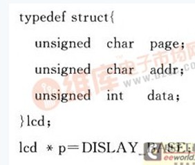
In the Nios II IDE environment, the program can be written by using the module added by itself, and the internal registers can be read and written by directly calling the IOWR (BASE, OFFSET, DATA) and IORD (BASE, OFFSET). This article uses the structure to define a pointer to the structure of the module, read and write operations on the register.
CBGl28064 itself does not have a font, you can add fonts in two ways: one is to make the required font into hardware ROM, increase the cost of hardware resources, and lack of flexibility; the other is to define the font in the software, by writing The data register is displayed. This design adopts the second method, defines the font in the software, and writes a simple display test program, displaying the word "ZHONG GUO" on the LCD screen. The test results show that the design is correct and feasible. In addition, the graphic data generated by the font software can also be displayed graphically.
Conclusion
In this paper, the finite state machine is used to design the CBGl28064 liquid crystal module driver hardware logic, and the display driver IP core is packaged to form a modular independent component, which can be reused in other projects; on this basis, based on NiosII embedding The processor builds a custom system-on-a-chip. Tested on the Cyclone series of FPGAs, the driver can display characters and graphics on the C-BGl28064 LCD module. The entire system reflects the flexibility and scalability of the SOPC embedded system.
Edit: Nizi
Capacitor for power transmission and transformation
Capacitor For Power Transmission And Transformation
New Parallel Capacitor 100Kvar,Capacitor Banks,High Voltage Capacitor Banks,Parallel Capacitor 200kar
YANGZHOU POSITIONING TECH CO., LTD , https://www.yzpstcc.com