Design of Automobile Shock Absorbing Spring Fault Diagnosis Instrument Based on DSP
This article refers to the address: http://
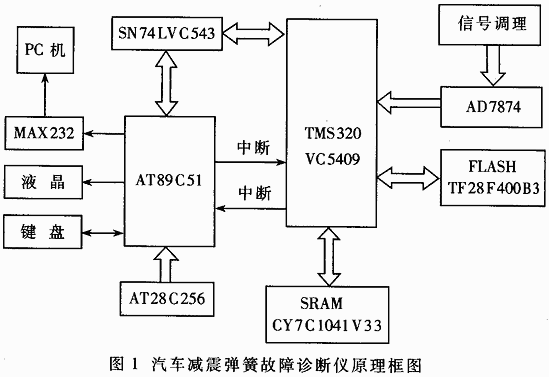
1 system overall plan
The nonlinear system identification algorithm is large and complex, and requires high computational power of the system. DSP is a chip specially used for digital signal processing. It has powerful computing power and fast computing speed, which can meet the requirements of the system. Although DSP's computing power is very strong, its event management capability is weak, and there are few I/O ports directly supported. In order to realize human-computer interaction conveniently, the method of working with DSP and single-chip microcomputer is adopted: the single-chip microcomputer is used as the host, and the DSP is realized through the communication interface; at the same time, the functions of human-machine interface and display are realized by using the strong peripheral device management capability of the single-chip microcomputer. The main work flow is: the input and output signals of the spring are conditioned by the filter circuit, and then converted into digital signals by the A/D converter, and then enter the DSP for calculation. The obtained diagnosis result is sent to the single-chip microcomputer through the communication interface circuit, and the result of the single-chip microcomputer is displayed. On the LCD, and through the serial port to the PC. The MCU controls the working state of the DSP through the communication interface. The system block diagram is shown in Figure 1.
2 hardware circuit design
2.1 Signal Conditioning Circuit
The integrated switching capacitor filter MAX280 is used to form an anti-aliasing filter circuit. The MAX280 is a fifth-order low-pass filter with adjustable cutoff frequency. When its clock pin is connected to the internal clock, the maximum cutoff frequency is 1.4 kHz. When the car damper spring is stable, the frequency of the signal does not exceed 500 Hz, so the cutoff frequency of the filter is set to 700 Hz.
2.2 DSP circuit
The DSP circuit completes data acquisition and digital filtering, and uses built-in algorithms to complete tasks such as fault diagnosis.
The DSP in this system uses the TMS320VC5409 produced by Texas Instruments (TI), which is a high-speed, cost-effective, low-power 16-bit fixed-point general-purpose DSP chip of the TMS320C54xx series. Key features include: improved Harvard architecture (1 program memory bus, 3 data memory buses and 4 address buses), dedicated hardware logic CPU, on-chip memory, 6-stage pipeline structure, on-chip peripheral-specific instructions set. The TMS320VC5409 contains 16K words of on-chip ROM and 32K words of on-chip DARAM. The program space has an address range of 8M, and the data and I/O space address range is 64K. The single-cycle instruction execution time is 10ns, dual-supply (1.8V and 3.3V), with JTAG boundary-scan simulation logic in accordance with IEEE1149.1.
The DSP circuit adopts 16-bit parallel self-boot mode. For the TMS320VC5409, the user program is stored in the external data space (8000H~FFFFH), so a FLASH ROM is expanded as a data storage space. FLASHROM uses INTE's TE28F400B3T90 (256K×16), which is divided into 15 blocks (8 4K words, 7 32K words), which can be erased separately. The programming voltage is only 3.3V and the fastest read speed is 90ns. The system expands a piece of SRAM as an external program space. The SRAM uses CYPRESS's CY7C1041BV33 (256K x 16) with an access speed of 10 ns.
2.3 A / D conversion circuit
Signal acquisition and conversion is done by the AD7874. The AD7874 is a 12-bit A/D converter manufactured by AD. The system requires the input and output signal phases to be synchronized. The AD7874 has a built-in sample and hold device that enables simultaneous sampling of four signals. Synchronous sampling minimizes the phase matching error of the system's input and output signals. The start of the A/D conversion is triggered by the rising edge, and after the four-way signal conversion is completed, an interrupt signal is generated. The sampling frequency of each channel can reach 29kHz. Since the A/D conversion outputs a TTL level and the DSP operates in a 3.3V signal environment, a level shifting circuit is required between the A/D output and the DSP input. Level conversion is implemented in this system using SN74LVC245. The Power Supply of the DSP system is completed by TI's voltage conversion module TPS767D318PWP, which can output two voltages of 3.3V and 1.8V.
2.4 single chip circuit
The single-chip circuit realizes keyboard input response and liquid crystal display and interaction with PC.
The single chip microcomputer used in this system is AT89C51 of ATMEL Company. Keyboard management is accomplished by keyboard controller 8279. The LCD module uses Truly's VPG12864T (128×64 dot matrix), which has a built-in T6963C controller that can work in text or graphics mode. The LCD display interface program is relatively large, so an AT28C256 is externally expanded as an external program memory. The level of the RS-232 serial port of the PC is not compatible with the TTL level of the serial port of the microcontroller, and the conversion between the two levels is completed using the MAX232.
2.5 Communication circuit
The communication circuit realizes the communication between the single chip and the DSP. Since the data communication between the microcontroller and the DSP is not large, an 8-bit bidirectional latch is used for data exchange. The bidirectional latch uses TI's SN74LVC543. When the DSP sends data to the AT89C51, it first latches the data in the SN74LVC543, then sends an interrupt to the AT89C51. The AT89C51 responds to the interrupt and removes the data from the latch. vice versa.
3 software design
The software design mainly includes DSP programming and microcontroller programming. The main task of the DSP program is to initialize, manage the DSP peripheral circuits and complete the algorithm for fault diagnosis. The MCU program includes a keyboard control program, a liquid crystal drive display program, and a program for communicating with a DSP and a PC.
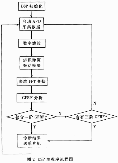
3.1 DSP main program
The main program flow chart of DSP is shown in Figure 2.
3.2 Download and boot of DSP programs
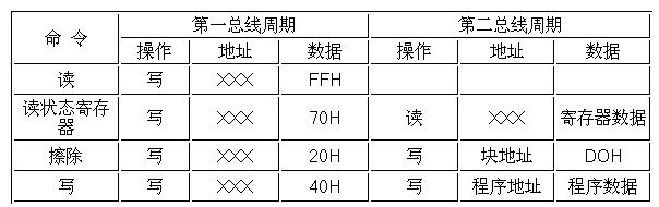
In this system, the FLASHROM is a TSOP package, soldered on the board, cannot be programmed by the programmer, and can only write the erase program by itself. Write the program code according to the format of the 16-bit parallel boot mode bootstrapping table (see Table 1), compile the link and download it to the DSP through the JTAG port; write the TE28F400B3 erase program to download the program to different locations in the DSP. Run the erase program, the program code is written to the FLASH. It should be noted that since the write speed of FLASH is slow compared with DSP, it is necessary to delay enough time after each word is written, otherwise the next word cannot be written normally. After writing, you need to reset the FLASHROM to read mode so that you can see the correct results in the development environment CCS. The maximum read speed of the TE28F400B3 is 90ns, while the TMS320VC5409 can only set up to 7 wait states. Therefore, set the CLKMD1, CLKMD2, and CLKMD3 pins of the DSP to make the system clock of the DSP at power-on reset 50MHz. This ensures reliable reading of FLASH data. After completing the boot process, the CLKMD register must first be cleared, then the CLKMD register must be reset to make the system clock 100MHz. The main operation commands of the TE28F400B3 are shown in Table 2.
Table 1 Code structure of 16-bit parallel boot mode
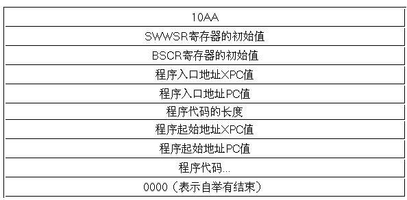
Table 2 Main operation commands of the TE28F400B3
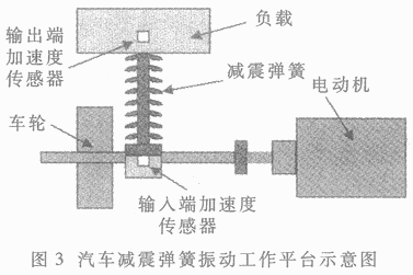
4 experimental system
The vibration spring experiment system is shown in Figure 3. The platform uses the real Santana 2000 suspension system and shock absorbing springs. The rotation of the motor is controlled by the frequency converter, and the wheel is rotated by the drive shaft. The lower end of the wheel is in contact with an iron bar having a rotatable surface mounted on the fixed bracket with a protruding rib. The wheel rotates to collide with the dam, and the suspension system causes the damper spring to vibrate accordingly.
Experiment with two good springs and three bad springs. The experimental results show that the automobile shock absorber spring fault diagnosis instrument works stably and the diagnosis result is effective.
The automotive shock absorber spring fault diagnosis instrument designed in this paper can be directly used for fault diagnosis of automotive shock absorber springs, and can be applied to nonlinear mechanical fault diagnosis such as bearing wear and brake failure. In this case, the fault diagnosis instrument has a slight modification to the circuit and can be used for fault diagnosis of higher frequency signal systems.
Micro Solar Inverter,Micro Solar Inverter,24Vdc Input Micro Solar Inverter,Micro Solar Inverter 220Vac 500W
MEAN WELL LED Driver / LED Power Supply,MEAN WELL AC / DC Switching Power Supply Co., Ltd. , http://www.nbledpower.com