
The explosive growth of mobile data is driving the development of new receiver architectures for communications infrastructure to achieve greater capacity and greater flexibility. The software-defined radio system will be the next-generation communication system based on a high-efficiency RF ADC that can sample on the antenna side while supporting a large dynamic range. These ADCs are designed with very advanced CMOS technology and use a time-interleaved (TIADC) architecture to achieve very high sample rates. The disadvantage of this architecture is the time-varying mismatch error, which requires real-time calibration. This paper introduces a new background calibration method for gain and timing mismatch error, which is implemented by a less complex digital signal processing algorithm.
This article refers to the address: http://
Dual TI ADC mismatch error
An effective way to increase the speed of the ADC is to have the two ADCs work in parallel, eliminating the need for a phase sampling clock. The inevitable small mismatch between sub-ADC transfer functions can lead to spurious harmonics that greatly degrade the actual dynamic range. This type of ADC has four types of errors: DC offset error, static gain error, timing error, and bandwidth error.
In practice, using digital calibration technology, the DC offset error is relatively simple to handle. Among them, bandwidth error is the most difficult to deal with, and generally needs to be eliminated through careful design and layout. In this article, we will focus on gain and timing error calibration as this is the main cause of the reduced dynamic range.
Recommended calibration method
In practice, the Nyquist bandwidth of the ADC is not fully used, and some of it is usually reserved specifically for the roll-off characteristics of the anti-aliasing filter. This free frequency band can be used to inject a constrained calibration signal. The calibration signal uses a sine wave because the sine wave easily generates a clean spectrum, so there are two main features that can be applied:
1. The amplitude can be kept small enough to avoid any effect on the dynamic range and provide good estimation accuracy. Tests have shown that the -40 dBFS to -35 dBFS level range is suitable for 14-bit ADCs.
2. The frequency is limited to the following discrete values ​​to reduce the complexity of the digital signal processing algorithm:
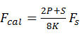
(Formula 1)
Where Fs is the TI ADC sampling frequency, P and K are unsigned integers, S = ±1, depending on the position of the calibration signal relative to the edge of the Nyquist zone (see Figure 1). The calibration signal can be easily generated on-chip by using a fractional-N PLL with the ADC clock as a reference signal. Choosing a sufficiently high K value, the harmonics of the calibration signal will alias outside the useful bandwidth, which will reduce the filtering requirements. The amplitude adjustment can be achieved with a programmable attenuator at the PLL output.
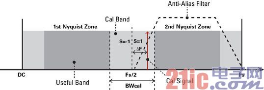
Figure 1: Frequency planning shows the location of the calibration signal. If x0 and x1 represent the outputs of the two sub-ADCs and the calibration signal is its input, Equation 1 can be used to represent them. The following expression connects the two signals (ignoring the noise):
(Formula 2)
The coefficients h0 and h1 of this linear filtering formula can clearly correspond to the gain g and the timing Δt error:
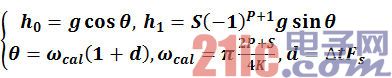
(Formula 3)
A first-order approximation can be used, and the mismatch error in the design is relatively small. This nonlinear equation is linearized and inverted.
The estimation algorithm consists of the following three steps:
1. Extract the calibration signal and use the LMS algorithm to remove it from the output of the sub-ADC to generate discrete-time signals x0 and x1. This algorithm requires the application of a digital cosine/sinusoidal reference signal at the calibration frequency. A small-scale lookup table (LUT) with a capacity of 4K (in practice, K < 64) is used to generate a cosine signal. A sinusoidal signal is generated by simply delaying the cosine signal by K.
2. As shown in Figure 2, the coefficients h0 and h1 are adaptively estimated from the extracted x0 and x1 signals using the LMS algorithm.
3. Calculate the gain and timing error from the linear equations given in Equation 3.
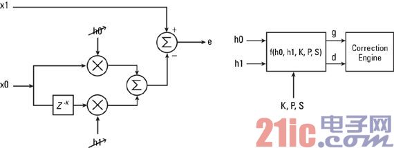
Figure 2: Gain and timing error background estimation using a 2-tap digital adaptive filter.
After the estimation results are obtained, the gain and timing errors are input to the digital calibration engine. The gain is compensated using a simple digital multiplier. The timing error is calibrated using a modified fractional delay filter. The complexity of the filter implementation is reduced by multiphase and symmetric methods. Both the estimation and calibration engines operate at the sampling rate of the sub-ADC. For further optimization, the estimation module can also use a downsampling scheme.
Method validation
All the synthetic test signals include: a 300 MHz one-way TM3.1, a 20 MHz LTE carrier, and a 253.44 MHz, -35 dBFS calibrated sine wave. Corresponding to S=1, K=8, P=2K, these signals can be generated using the test setup in Figure 3. This setup has a low noise and high linearity D/A converter and DVGA, so its dynamic range is very high. We use a commercial 14-bit/500Msps TIADC that integrates high-resolution adjustable gain and timing error. The ADC raw data is acquired by the FPGA, and the data is processed by the IDT calibration algorithm using Matlab software. The gain and timing errors of the TI ADC are set to approximately 0.5 dB and 5 ps, respectively, to simulate the worst case.
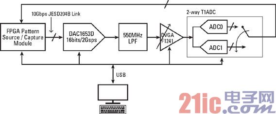
Figure 3: Test setup diagram. Figure 4 shows the data power spectrum before and after calibration. The LTE carrier image is -80 dBFS before calibration and is reduced by approximately 30 dB to -110 dBFS after calibration. The extraction and cancellation algorithms completely eliminate the calibration signal and its image. This performance was obtained during a convergence time of approximately 200 μs.
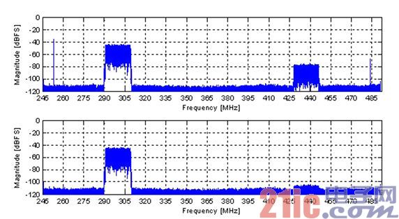
Figure 4: Power spectrum before (top) and after calibration (bottom) with a 300 MHz LTE carrier.
The calibration signal remains unchanged and the LTE carrier center frequency is swept from 50 MHz to 400 MHz to assess frequency behavior. As shown in Figure 5, the resulting image rejection indicates that the dynamic range is increased by at least 30 dB in both first Nyquist zones. As expected, if the bandwidth error is not calibrated, the frequency is limited, resulting in reduced image rejection.
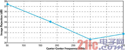
Figure 5: Image rejection versus LTE carrier center frequency comparison using a fixed calibration signal.
in conclusion
The RF sampling A/D converter is a key component of the next generation software radio system. With a time-interleaved architecture, very high sample rates and low power consumption can be achieved at the expense of dynamic range degradation. As can be seen from the foregoing, injecting constrained calibration signals outside of the used bandwidth and using less complex algorithms to calibrate the gain and timing errors can significantly increase the dynamic range. Measurements of the 14/500 Msps prototype show that the dynamic range of the two first Nyquist zones is approximately 30 dB higher. This proposed method can be used for higher speed applications as long as the gain/timing mismatch error model remains valid.
Aluminium Train Body And Interior
Aluminium Train Body,Aluminium Train Interior,Slot Aluminum Extrusions,Aluminium Corrugated Sheet
KAM KIU ALUMINIUM GROUP , https://www.kamkiualuminium.com