
1 Introduction
Image acquisition is the basis of digital image processing, image recognition and machine vision, and its application fields are very extensive. The optical image is mainly converted into a digital signal by using a photoelectric conversion device such as CCD or CMOS, and then the data is input into the processor through the corresponding interface for digital analysis and processing of the image. The MV-D1024E is a CMOS-based high frame rate series camera with a CAMERA-LINK interface. CAMERA-LINK is a high-speed data connection protocol for Dingye applications that provides a simple, flexible communication interface between digital cameras such as CCD or CMOS and image acquisition systems.
Under normal circumstances, the image acquisition system is based on digital cameras such as CCD or CMOS. It also needs a capture card to complete data acquisition. Common acquisition cards are based on DSP implementation and FPGA-based. MV-D1024E series cameras are also available from manufacturers. The acquisition card, which receives the data of CAMERA-LINK, is simply processed by the acquisition card. Data is transferred to the PC via the PCI bus. However, such a data acquisition method based on the PCI bus has certain defects, and the data can only be connected to the PC through the PCI interface, and the image processing function can only be completed by the PC. So that the system can not run away from the PC, in many image processing applications, it needs to be separated from the PC, and the system is required to be small in size, light in weight, low in power consumption and good in portability. With the wide application of programmable logic devices, field programmable gate arrays (FPGAs) are widely used in high-speed real-time image acquisition systems due to their advantages of high reliability, high integration, low power consumption and high computing speed. Here, the FPGA is used to control the data interface of the MV-D1024E series camera, which realizes the function of the image acquisition card from the PC. To facilitate system and user input, a USB-based PC interface was designed. It can also be used to disconnect the PC from the USB interface.
2 image acquisition system block diagram
The image acquisition system consists of CAMERA-LINK interface, USB communication interface control, camera control and camera data buffer storage control module. The system block diagram is shown in Figure 1.
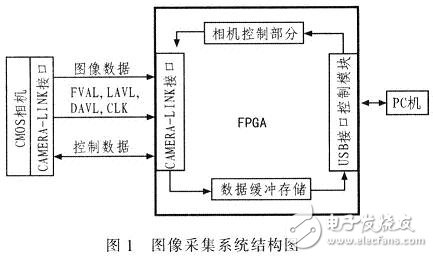
The core controller uses Altera's Cyclone series EPlC6Q240C8. The parameters such as the exposure time, frame rate and display window size of the camera are set by the PC, and the control command is transmitted by the USB to the USB interface control module in the FPGA, and the integrated camera control module according to the received parameters will have been The control code corresponding to the camera solidified in the internal ROM of the FPGA is transferred to the CAMERA-LINK module for processing, and then the control code is sent to the camera through the internal serial module. After the camera gets the control command, it starts working. The CAMERA-LINK module encapsulated in it sends the image data, clock signal, frame rate signal, horizontal frequency signal and data valid signal to the CAMERA-LINK module of the FPGA, and passes through the FPGA. The data buffer memory module performs a ping-pong operation on the high-speed data stream, and then transfers the data to the PC display and storage processing.
3 image acquisition system design
3.1 Introduction to EP1C6Q240C8
The FPGA master device is the EP1C6Q240C8 of Ahra's Cvclone series, with 5 980 logic cells and 120,000 typical gate resources and 185 programmable I/O ports. The maximum operating clock can be above 300MHz, and the core supply voltage is 1.5V. The I/O buffer supply voltage is 3.3 v, and the system configuration is realized through the JTAG interface. The configuration device used EPC4 serial ROM capacity is about 4 Mbit, can be reprogrammed about 50 times, JTAG interface is IEEE Std. 1149.1 standard.
3.2 Introduction to MV-D1024E Camera and CAMERA-LINK Interface
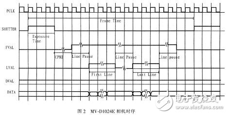
The MV-D1024E is a high-speed, high-dynamic CMOS camera series featuring CMOS active pixel technology with 12-bit sampling resolution and 1 024 & TImes; 1 024 pixel resolution at which frame rate can reach 150 frames per second. The exposure time is adjustable from 10 μs to 0.41 s in 25 ns steps. The camera is configured with a serial port using the CAMERA-LINK interface. CAMERA-LINK is an extension of National Semiconductor's Channel Link technology for driving flat panel displays. It has a very high transfer rate of up to 1 Gb/s, providing high resolution and digital data at various frame rates, data output. Adopt LVDS format, fast speed and good anti-noise. According to the application requirements, it supports basic (Base), Medium (Medium), All (Full) and other digital formats, the interface has an open interface protocol, compatibility is good. It is suitable for communication interfaces between digital cameras such as CCD or CMOS and image acquisition systems. As shown in Figure 2, when FVAL, LVAL, and DVAL are both high, there is data on the data master route at the rising edge of the camera clock PCLK.
3.3 Camera interface and control module design
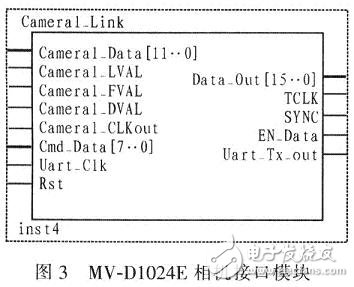
The MV-D1024E series camera has a 12-bit data output, an additional camera clock PCLK, a frame rate signal FVAL, a horizontal frequency signal LVAL, and a data valid signal DVAL. Figure 3 shows the camera interface module generated by the FPGA design. The module completes the camera data and the access of each clock signal, and integrates the serial interface module to send the user's control signal to the camera to the camera. Complete the camera's parameter setting function.
| About Glass Fiber Film Covered Flat Aluminium Wire |
Flat Fiber glass wrapped Aluminium Wire for winding machine
Copper or Aluminum rectangular Wire
Narrow side size a : 0.80mm-5.60mm
Broad side size b : 2.00mm-16.00mm
Copper or Aluminum Round Wire
Diameter:φ1.7-φ5.0
If specification is out of range, please

Glass Fiber Film Covered Flat Aluminium Wire
Flat Copper Wire,Glass Fiber Film Covered Flat Aluminium Wire,Flat Aluminium Wire,Glass Film Covered Flat Wire
HENAN HUAYANG ELECTRICAL TECHNOLOGY GROUP CO.,LTD , https://www.huaonwire.com