
Central issue:
This article refers to the address: http://
Explore the design of 24VDC-220VDC vehicle Switching Power Supply
solution:
Designing the corresponding push-pull transformer by AP method
Push-pull inverter-high frequency transformer-full bridge rectification scheme
With the increase in the types of electric vehicles used in modern automobiles and the increase in power levels, more and more types of power supplies are required, including AC power and DC power. These power supplies need to use a switching converter to boost the +12VDC or +24VDC DC voltage provided by the battery to +220VDC or +240VDC through the DC-DC converter, and then convert the DC-AC converter to a commercial frequency AC power supply through the DC-AC converter. Frequency conversion voltage supply. For the pre-stage DC-DC converter, the high-frequency DC-AC inverter part, the high-frequency transformer and the AC-DC rectification part are included, and different combinations are adapted to different output power levels, and the conversion performance is also different. Push-pull inverter circuit has been widely used due to its simple structure and high utilization of transformer core, especially in low- and high-current input medium and small power applications. At the same time, full-bridge rectifier circuit also has high voltage utilization and support output power. High-level features, therefore, this paper uses a push-pull inverter-high-frequency transformer-full-bridge rectification scheme to design a DC-DC converter with 24VDC input-220VDC output and rated output power of 600W, and adopts the AP method to design the corresponding push-pull transformer.
1, the working principle of push-pull inverter
Figure 1 shows the basic circuit topology of a push-pull inverter-high frequency transformer-full bridge rectifier DC-DC converter. By controlling the two switching tubes S1 and S2 to be alternately turned on at the same switching frequency, and the duty ratio d of each of the switching tubes is less than 50%, a certain dead time is left to avoid simultaneous conduction of S1 and S2. The front-stage push-pull inverter inverts the input DC low voltage into an AC high-frequency low voltage, sends it to the primary side of the high-frequency transformer, and couples it through the transformer to obtain the AC high-frequency high voltage on the secondary side, and then passes the reverse fast The full bridge is rectified and filtered by the recovery diode FRD to obtain the desired DC high voltage. Since the back pressure that the switch can withstand is at least twice the input voltage, that is, 2UI, and the current is the rated current, the push-pull circuit is generally used in low- and medium-power applications where the input voltage is low.
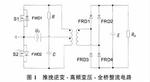
When S1 is turned on, its drain-source voltage uDS1 is only the turn-on voltage drop of a switching transistor. In the ideal case, uDS1=0 can be assumed, and at this time, an induced voltage is generated in the winding, and according to the same name of the primary winding of the transformer. In the end relationship, the induced voltage is also superimposed on the off S2, so that the voltage that S2 receives when turned off is the sum of the input voltage and the induced voltage is about 2 UI. In practice, the leakage inductance of the transformer will be large. The spike voltage is applied across S2, causing large turn-off losses. The efficiency of the converter is not very high due to the leakage inductance of the transformer. An RC snubber circuit, also called an snubber circuit, is connected between the drains of S1 and S2 to suppress the generation of spike voltage. And in order to provide a feedback loop for energy feedback, the freewheeling diode FWD is anti-parallel across S1 and S2.
2, the design of the switching transformer
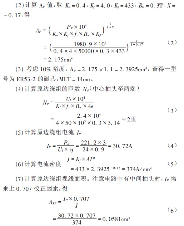
The area product (AP) method is used for design. For the push-pull inverter working switching power supply, the primary side supply voltage UI=24V, the secondary side is the full-bridge rectifier circuit, the expected output voltage UO=220V, the output current IO=3A, the switching frequency fs=25kHz, the initial transformer efficiency η= 0.9, working magnetic flux density Bw = 0.3T.
(1) Calculate the total apparent power PT. Set the voltage drop of the reverse fast recovery diode FRD: VDF=0.6*2=1.2V
3. Analysis of the problem of push-pull inverter
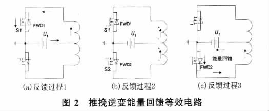
3.1 Energy feedback
During the conduction of the main circuit, the primary current increases with time, and the conduction time is determined by the drive circuit.
Figure 2 (a) is the equivalent circuit when S1 is turned on and S2 is turned off. The arrow in the figure is the current flow direction, flowing out from the positive pole of the power supply UI, flowing into the negative pole of the power supply UI through S1, that is, the ground, FWD1 is not conducting at this time; When S1 is turned off, before S2 is not turned on, the terminal voltage of S1 will rise due to the storage of primary energy and leakage inductance, and the terminal voltage of S2 will decrease by transformer coupling. At this time, the energy recovery in parallel with S2 is restored. The diode FWD2 is not yet turned on, and no current flows through the circuit until an induced voltage is generated on the primary winding of the transformer. As shown in Fig. 2(b); FWD2 is turned on, and the flyback energy is fed back to the power supply. As shown in Fig. 2(c), the arrow points in the direction of energy feedback.
3.2 waveform analysis of each point
When the falling edge of a PWN signal comes, the switching element of its control is turned off. Due to the storage of the primary side energy and the leakage inductance, the drain generates a surge voltage, which is greater than 2UI because the RC snubber circuit is added to make it final. Stable around 2UI.
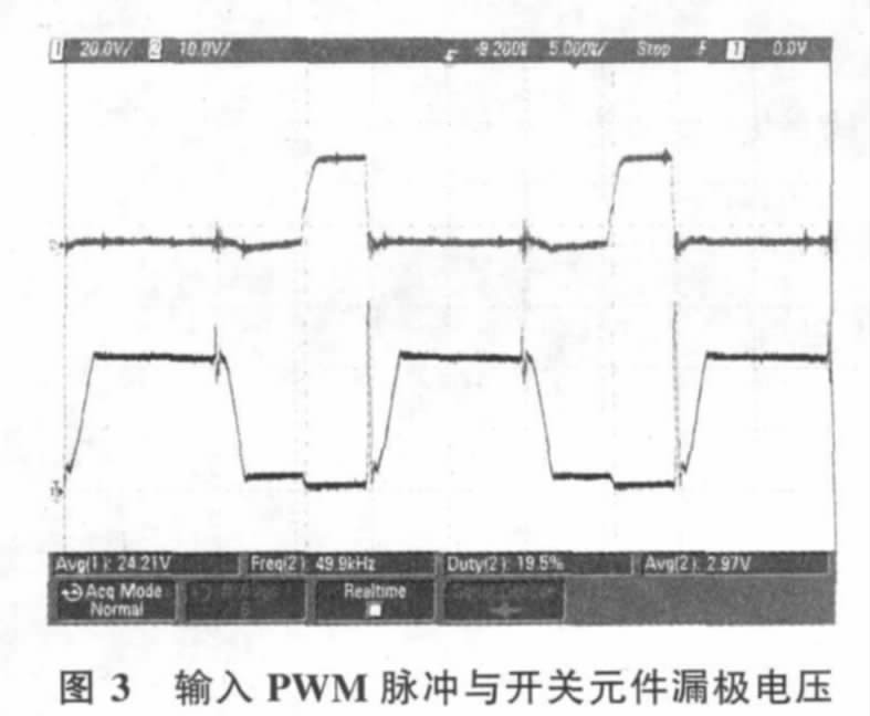
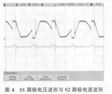
When the falling edge of the PWN signal of S1 comes, S1 is turned off, the drain generates a high surge voltage, and the feedback energy diode FWD2 connected in parallel with S2 is turned on to form an energy feedback loop, and the S2 drain generates a high impact. Current, see Figure 4.
4. Experiment and analysis
4.1 Principle design
Figure 5 shows the simplified main circuit. Input 24V DC voltage, after large capacitance filtering, connected to the middle tap of the primary side of the push-pull transformer. The other two taps on the primary side of the transformer are connected to two fully-controlled switching device IGBTs, and an RC snubber circuit is added between them to form a push-pull inverter circuit. The output of the push-pull transformer is rectified by full bridge, and the large capacitor is filtered to obtain 220V DC voltage. And the feedback voltage signal UOUT is obtained through the voltage dividing branch.
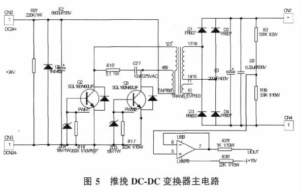
The CA3524 chip is used as the core to form a control circuit. The switching frequency of the fully-controlled switching device is adjusted by adjusting the resistance and capacitance values ​​between the 6 and 7 pins. The 12 and 13 pins output PWM pulse signals, and alternately control two fully-controlled switching devices through the driving circuit. The voltage feedback signal is input to the 1 pin of the chip. The reference voltage of the voltage feedback signal is input to the 2 pin by adjusting the potentiometer P2, and the PI regulator is combined with the 9 pin COM terminal together with the CA3524 internal operational amplifier to adjust the PWM pulse duty. Than to achieve the purpose of stabilizing the output voltage of 220V.
4.2 Results and analysis
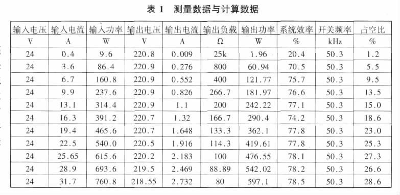
On the surface of the experiment, the output voltage is stable at 220V and the ripple voltage is small. The maximum output power can reach nearly 600W, and the system efficiency is basically stable at 80%, achieving the expected results. Among them, due to the large efficiency loss of IGBT, the system efficiency is low. Considering the use of MOSFET with low loss, the system efficiency will increase by at least 10%~15%.
Precautions:
(1) When the primary winding of the transformer is excited in the positive and negative directions, the corresponding volt-second product is not equal, which will cause the working magnetization curve of the magnetic core to deviate from the origin. This polarization phenomenon is related to the selection of the switch tube. The difference in reverse recovery time of the switch can result in a difference in the volt-second product.
(2) In the experiment, as the input voltage increases slightly, the system loss increases. The main reason is that the transformer core generates large eddy current loss, and the system efficiency decreases. The measures to reduce the eddy current loss mainly include: reducing the induced potential, such as using iron powder core material; increasing the electrical resistivity of the core, such as using ferrite material; and extending the path of the eddy current, such as silicon steel sheet or amorphous ribbon.
5 Conclusion
The push-pull circuit is especially suitable for small and medium power applications with low voltage and high current input, and a high frequency push-pull transformer is designed by the AP method. The experimental results show that the push-pull inverter-high-frequency transformer-full-bridge rectification scheme achieves the expected effect, so that the output voltage is stable at 220V and has a certain output hardness, and the efficiency reaches 80%, which provides a development for modern automotive power supply. A certain space for development.
Our Constant Current Led Driver /Lighting Power Supply range offers currents from 100mA to 8000mA; LED lighting driver offer high efficiencies, PFC, are available with Class P Input; IP ratings against dust and moisture from IP20 through to IP67 and protection for short circuit, over voltage, overload and over temperature conditions. With additional options such adjustable outputs and PWM, 1-10V, Resistive or triac dimming functions. Application fits for Led High Bay Light ,Industrial Led Lighting. High Power Led Driver .
We have skilled engineers to answer all your questions and enquiries and provide all-round solutions basis on your project(s) and provide technical supporting.
Paraneter:
Input voltage: 100-277vac / 100-240vac / 100-130vac / 180-240vac / 100-347V
output voltage: 25-40vdc / 27-42vdc / 35-45vdc / 50-70vdc / 12Vdc / 24vdc
current: 100mA-8000mA.
Power factor: >0.9
Dimming:0-10V / PWM / RX / DALI.
>=50000hours, 3-5 years warranty.
certificate: UL CE FCC TUV SAA ect.
What's the benefits of Fahold Driver?
- Standard Linear Lighting
- Cost-effective Led Driver solution for industry,commercial and other applications
- Good quality of led driver with high efficiency output to meet different requirements
- Easy to order and install,requiring less time,reducing packaging waste and complexity
- Flexible solution
-
FAQ:
Question 1:Are you a factory or a trading company?
Answer: We are a factory.
Question 2: Payment term?
Answer: 30% TT deposit + 70% TT before shipment,50% TT deposit + 50% LC balance, Flexible payment
can be negotiated.
Question 3: What's the main business of Fahold?
Answer: Fahold focused on LED controllers and dimmers from 2010. We have 28 engineers who dedicated themselves to researching and developing LED controlling and dimming system.
Question 4: What Fahold will do if we have problems after receiving your products?
Answer: Our products have been strictly inspected before shipping. Once you receive the products you are not satisfied, please feel free to contact us in time, we will do our best to solve any of your problems with our good after-sale service.
Constant Current Led Driver
Led High Bay Light,Industrial Led Lighting,High Power Led Driver
ShenZhen Fahold Electronic Limited , https://www.fahold.com