
1 Introduction
With the increasingly fierce competition in the mobile phone market, multimedia mobile phones have gradually become the darling of the market. Because there is a large amount of multimedia data, mass storage is the primary problem to be solved by multimedia mobile phones.
NOR and NAND are the two main non-volatile flash technologies on the market today. The NOR features on-chip execution (XIP, eXecuteInPlace) so that applications can run directly in flash memory without having to read the code into system RAM. The transmission efficiency of NOR is very high, and it is very cost-effective in a small capacity of 1 to 4 MB, but the low write and erase speed greatly affects its performance. The NAND structure provides extremely high cell density, high memory density, and fast write and erase speeds, making it an excellent choice for large data storage. When choosing a storage solution, the designer must consider the following factors:
(1) The reading speed of NOR is slightly faster than NAND.
(2) NAND write speed is much faster than NOR.
This article refers to the address: http://
(3) NAND's 4ms erase speed is much faster than NOR's 5s.
(4) Most write operations require an erase operation first.
(5) The erase unit of NAND is smaller, and the corresponding erase circuit is less.
(6) The maximum number of erasures per block in NAND flash is one million, and the number of times of NOR is 100,000.
In addition, the use of NAND is much more complicated than the use of NOR. No software support is required to run code on a NOR device. When doing the same on a NAND device, a driver, usually a memory technology driver (MTD), is used for NAND and NOR devices during write and erase operations. All need MTD.
There are relatively few MTDs required to use NOR devices. Many vendors offer more advanced software for NOR devices, including M-SySTem's TrueFFS driver, which is powered by WindRiverSystem, Microsoft, QNXSoftwareSystem, Symbian and Intel. Adopted.
2 TC58DDM82A1XBJ5 application in multimedia mobile phones
In multimedia mobile phones, TC58DDM82A1XBJ5 is mainly used to store files with large data volume such as pictures and sound files.
TC58DDM82A1XBJ5 is a 256Mbits NAND EEPROM produced by Toshiba. The operating voltage is 2.7V~3.6V or 1.65V~1.95V.
The storage structure is 528 bytes × 32 pages × 2048 blocks. The size of the Page is 528 Bytes, and the size of the Block is (16K + 512) Bytes.
2.1 Pinout and function
NANDFlash uses a highly multiplexed access interface that acts as both an address bus and a data bus and instruction input interface. The interface pins of NANDFlash are mainly divided into three categories: data pins, control pins, and status pins. The data pins of the TC58DDM82A1XBJ5 are 8-bit, ie I/O1~I/O8, used to input/output addresses, data and instructions. There is a status pin (RY/BY) to indicate the state of the chip. When the chip writes, erases, or reads randomly, its output level is high, indicating that the chip is busy, otherwise it outputs low level. . The /WP pin is used to disable the write operation of the chip. Write operation is disabled when it is low, otherwise write operation is allowed. There are 6 control pins, see pin definitions.
2.2 Connection of TC58DDM82A1 and AD6528
The AD6528 is a Hermes series GSM/GPRS processor from Analog Devices Inc. The AD6528 uses a dual-core architecture of DSP+MCU, in which the MCU is ARM7, and the DSP part uses ADI's own ADSP-218xDSP core.
2.3 How to Operate the TC58DDM82A1
The address input, command input, and data input and output of the TC58DDM82A1 are controlled by CLE, ALE, CE, WE, RE, RST, and PRE1/PRE2 pins. The control logic is shown in Table 1:
Table 1 logical table 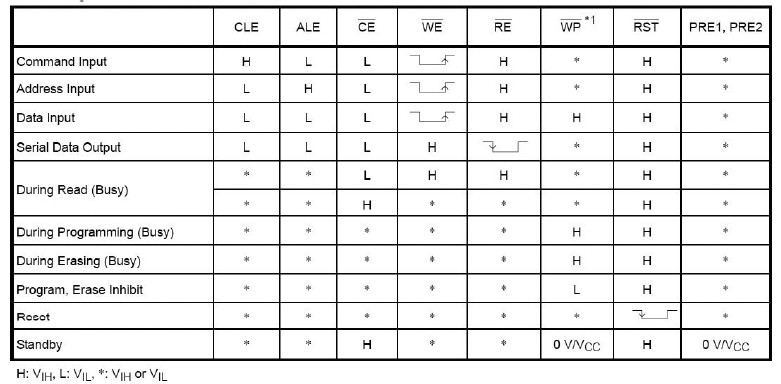
*1: /WP=0, prohibits Program and Erase operation of TC58DDM82A1. The various working modes of TC58DDM82A1, such as read, reset, and program, are controlled by command words.
2.4 Timing Analysis and Driver of TC58DDM82A1
It can be seen that in the first cycle, when the CLE signal is valid, the command 00H is sent to the command register through the IO port. At this time, the NANDFlash is in the write state, so the WE is valid and the RE is invalid. After sending the command, it then sends the address to be read, which will take up 3 cycles of WE. Note that the address information is sent at this time, so CLE is low and ALE is high. When the information is sent, the data cannot be read immediately, because the chip is in the BUSY state and needs to wait for 2~20ms. After that, the real data reading can be started. At this time, WE is at a high level and is in an inactive state, and the CE chip select signal is always low to indicate that the chip is selected.
The pseudo code for completing ReadMode(1) is as follows:
ReadMode1_Func(Cmd, Addr)
{
RE=1;
ALE = 0 ;
CLE = 1 ;
WE = 0 ;
CE=0;
SendCmd(Cmd); // Send an operation command to NAND, in this case it should be 00H
WE = 1 ; / / NAND take command
CE = 1 ;
CLE=0; // send command ends
ALE=1; // start sending the start address
For(i=0;i<3;i++)
{
WE = 0 ;
CE=0;
SendAddr(Addr);
WE=1; // Take the instruction
CE=1;
} // Send all addresses
CE=1;
WE = 1 ;
ALE = 0 ;
Delay(2);
While(BUSY)
Wait; // Determine if the wait state is over
RE=0;
CE=0;
ReadData(Buf); // read data to buffer
}
2.5 NANDFlashDiver special features
The access of NANDFlash is serial, which is similar to the storage method of hard disk. NANDFlash must have Driver support in order to use it on your phone. In addition to providing Read, Program, and Erase for NANDFlash, Driver should also provide the following basic functions:
BadBlockManagement
WearLevelingTreatment
ECC (ErrorCorrectCode)
NANDFlash is accessed through the logical address assigned by the Driver. BadBlockManagement does not assign logical addresses to bad blocks, which creates a continuous logical address. WearLevelingTreatment avoids a lot of read and write operations on a certain area, which will extend the usage time of NANDFlash. ECC mainly corrects errors during reading and writing, but ECC can only correct 1 bit of data.
3 Conclusion
In multimedia mobile phones, NANDFlash is mainly used to store multimedia data (pictures, voice files, etc.). In actual applications, NANDFlash is not frequently written and erased, and the integrity requirements of multimedia data are not high, but the amount of data of multimedia data is large. These characteristics determine the use of NANDFlash to store multimedia data is very appropriate, which is the industry's common practice.
In China, as a manufacturer and supplier of Switching Power Supply, we are seeking truth from facts, focusing on product quality and providing the best service to customers.We have experienced engineers to develop products, supervise the quality of products.Our Power Supply 100% full load test before shipment,and with safe packing.We can make the power supply meet every clients needs.
19V Switching Power Supply,19V Dc Power Supply,Power Supply 19V,19V Power Supply
Shenzhen Pengchu Industry Co., Ltd , https://www.pc-adapters.com