
A signal generator system based on DDS chip AD9850 and single-chip AT89S52 is studied, which can generate three waveforms of sine wave, triangle wave and square wave. The frequency and amplitude of the system can be adjusted numerically. Compared with the performance of traditional signal generators, it has the advantages of frequency bandwidth, stable frequency, good waveform, simple interface, convenient programming, low cost and easy miniaturization.
1 The basic principle of DDS technology The principle block diagram of the sinusoidal signal generator implemented by the DDS method, as shown in Figure 1, is mainly composed of a phase accumulator, a phase modulator, a sinusoidal ROM lookup table, a D / A converter, and a low-pass filter. The phase accumulator is the core of the entire DDS and completes the phase accumulation operation. DDS technology is to sample the sinusoidal signal according to the phase interval and store the resulting waveform data in a customized sinusoidal ROM table. During frequency synthesis, the phase accumulator counts the clock pulses under the action of the reference clock, and at the same time adds the accumulated phase output by the accumulator and the phase increment preset by the frequency word input to form a sinusoidal lookup table with the added result Address; take out the waveform data value in the unit corresponding to the phase in the table, the analog signal is output by the D / A converter, and then the waveform is smoothed by the low-pass filter to obtain an analog signal that meets the requirements.
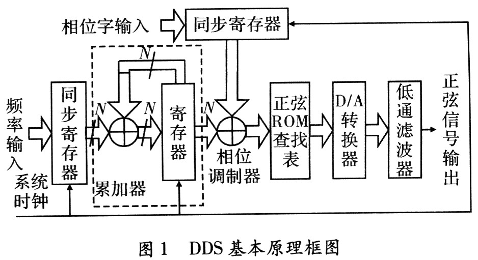
The phase accumulator is formed by a cascade of N-bit word adders and N-bit accumulation registers. The adder can accumulate the binary code of the frequency word input. The accumulation register is a typical feedback circuit, and the accumulated result is used as a sine The next sampling address value of the ROM lookup table sends the data taken from the waveform table to the D / A converter for conversion, and finally outputs a sinusoidal signal through the filter circuit. The maximum count length of the phase accumulator is the same as the number of phase separation points stored in the sine lookup table. Due to the different phase increments of the phase accumulator, the number of sampling points within a week will be different, so that the frequency of the output signal will also change accordingly (realization frequency conversion). If the initial phase of the accumulator is set, the output signal can be phase-controlled. It can be seen from the sampling principle that if two identical frequency synthesizers are used, and their reference clocks are the same, and the same frequency word input and different initial phase are set at the same time, then in principle, it is possible to realize that the output two channels have a certain phase The possibility of a poor co-frequency signal effectively solves the problem of phase asynchronization in general communication channels, which is also a significant advantage of DDS technology.
Basic DDS commonly used parameter calculation formula, the output frequency is ![]() ; Frequency resolution is
; Frequency resolution is ![]() ; Frequency word input is
; Frequency word input is ![]() ; Phase resolution, that is, the minimum phase step is
; Phase resolution, that is, the minimum phase step is ![]() . Among them, B △ θ is the phase increment (frequency word); fout is the signal output frequency; fclk is the clock frequency: D is the address width of the table.
. Among them, B △ θ is the phase increment (frequency word); fout is the signal output frequency; fclk is the clock frequency: D is the address width of the table.
As long as the phase quantization value is accumulated, the current phase value of the sinusoidal signal can be obtained; and the phase increment quantization value BΔθ used for accumulation determines the signal output frequency fout, and presents a simple linear relationship. Direct digital frequency synthesis technology is a digitally controlled frequency synthesizer designed based on the above principles.
2 System hardware circuit design
2.1 Introduction of AD9850 chip AD9850 is a highly integrated DDS chip produced by American AD company, using CMOS process, its power consumption is only 155 mW when 3.3 V power supply, extended industrial temperature range is -40 ~ 80 ℃, Use 28-lead SSOP surface package. The composition principle of the chip is shown in Figure 2. The inner dotted line is a complete programmable DDS system. The outer dotted line contains the main components of the AD9850. The AD9850 contains a programmable DDS system and a high-speed comparator, which can realize frequency synthesis controlled by all digital programming.
Under the 125 MHz system clock, the 32-bit frequency word input in the AD9850 can make the frequency resolution of the output signal reach 0.029 Hz, and has a 5-bit phase word input, allowing the phase to be increased by 180 °, 90 °, Adjust at 45 °, 22.5 °, 11.25 ° or a combination of these values. The chip performs direct digital synthesis on the input standard sine wave. The maximum input signal frequency is fclk = 125 MHz, which can generate sine and square waves of any frequency within the range of 0 to fclk / 2. After the AD9850 is connected to the clock circuit, it can generate an analog sine wave output with programmable frequency and amplitude. This sine wave can be used directly as a signal generator or converted into a square wave output through an internal high-speed comparator.
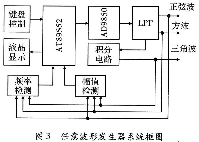
2.2 Hardware circuit design The signal generation system is based on the single-chip AT89S52 as the controller and the DDS chip AD9850 as the core, and the corresponding signal output is generated by the single-chip control function chip to achieve frequency presetting and control word setting. AD9850 realizes the function of a signal generator, and the microprocessor controls the D / A converter to realize the adjustability of various signal amplitudes. The hardware circuit of the entire signal generation system is mainly composed of five parts: a single chip microcomputer and peripheral control circuits, a sine signal generator function circuit, an integration circuit, a filter circuit, and a detection circuit. The system block diagram is shown in Figure 3. Among them, the keyboard uses a 4 × 4 matrix type, which is mainly used to set the frequency and amplitude; the waveform uses LCDl602 liquid crystal display; the LPF low-pass filter and integration circuit are implemented by the analog integrated chip LM324.
3 System software design The system software design uses assembly language and C language to write the program, which not only improves the controllability of the program to the circuit hardware, but also increases the readability and portability of the program. The software module includes four parts: main program (AT89S52 initialization, AD9850 initialization, LCDl602 initialization), display subprogram, keyboard input subprogram, signal generation and control subprogram. The main program flow of the signal generator system is shown in Figure 4.

4 Experimental research and data analysis According to the idea of ​​system design, hardware circuit construction, hardware debugging, software debugging and joint debugging of prototype are carried out. Use the EEl64lC function signal generator, YB217-3B dual digital millivoltmeter, EZl DS2250 digital oscilloscope and other equipment provided by the electronic laboratory to test the developed signal generator. The experimental results of sine wave frequency and amplitude are shown in Table 1 and Table 2, the experimental results of triangular wave frequency and amplitude are shown in Table 3 and Table 4, and the experimental results of square wave frequency and amplitude are shown in Table 5 and Table 6 Show.
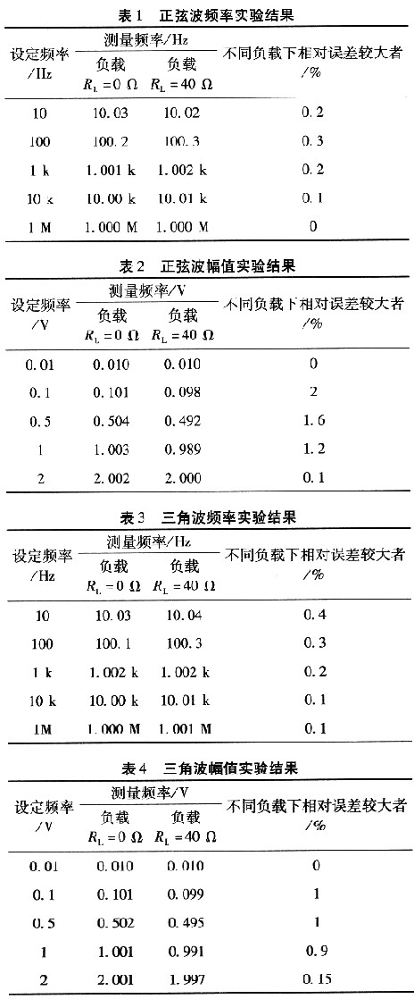

It can be seen from the experimental results that the relative errors of the sine wave, triangle wave and square wave generated by the signal generator system are less than 0.5%, and the relative errors of the amplitude are less than 5%, which meets the design requirements .
5 Conclusion The frequency and amplitude of the DDS technology can control the arbitrary waveform generator system. The results show that the signal generator system software and hardware circuit design is correct and reliable, with frequency modulation and amplitude modulation functions. The phase control of the signal generator needs further study.
Mini Circuit breakers, also named as the air switch which have a short for arc extinguishing device. It is a switch role, and also is a automatic protection of low-voltage electrical distribution. Its role is equivalent to the combination of switch. Fuse. Thermal Relay and other electrical components. It mainly used for short circuit and overload protection. Generally, According to the poles, Mini Circuit Breaker can be divided into 1P , 1P+N , 2P, 3P and 4P.
Miniature Circuit Breaker,Electronics Miniature Circuits Breaker,Automatic Miniature Circuit Breaker,Mini Circuit Breaker
Wenzhou Korlen Electric Appliances Co., Ltd. , https://www.korlenelectric.com