
Power Systems
This article refers to the address: http://
The power system is one of the most important subsystems in any automotive system design. Overall power consumption, battery reverse polarity protection, vehicle tripping, vehicle noise, and vehicle sleep power are all factors that must be considered. If the power supply design is bad, then even the best system will not work. Motorola's intelligent power semiconductor products provide excellent management of all aspects of the power subsystem.
Motorola's System-on-Chip (SBC) MC33989 has two power rectifiers that power the MCU and peripherals. An on-chip CAN interface with 1 megabaud, four high-voltage wake-up inputs, and system protection are also available. This intelligent semiconductor device provides all the necessary system voltages and has a low noise 200mA rectifier inside to power the MCU subsystem. In addition, there is a device that controls the external conduction transistor to supply power to peripheral devices. This external turn-on transistor allows the secondary supply to be adjusted to meet the power dissipation requirements of each particular application. The secondary power supply can also cut off the power supply of the selected peripheral device as required, thereby reducing power consumption.
The input power comes directly from the car battery. Simply add an external diode to achieve battery polarity protection. The SBC can perform protection actions under all overvoltage conditions. The application of the power MOSFET process technology also enables the device to operate normally when the battery voltage is as low as 4.5V, and can output a battery failure alarm signal when the battery voltage is as low as 3V. The power system also has an over-temperature protection function that will perform internal thermal shutdown when the temperature reaches 160 degrees Celsius, and an alarm signal will be output when the temperature is 130 degrees Celsius. In addition, the SBC provides a low-power sleep mode in which the system's current can be reduced to 40μA.
CAN transceiver
In addition to providing system power, the SBC also integrates a 1 megabaud CAN transceiver. The transceiver features master status timeout detection, internal thermal protection, and CAN+ and CAN-input short-circuit protection. The transceiver also internally trips the CAN+ and CAN- inputs, reverses the battery, and shorts to power or ground protection.
Four high-voltage wake-up inputs give the device a powerful wake-up function. These wake-up inputs have a maximum withstand voltage of 40V. The pull-up source at the input can be generated on the chip. Since the change of the switch input can be detected at any time by simply pulling up the source, the power consumption can be well reduced. The device also features a periodic wake-up function. In addition, the SBC also provides reset adjustment and low-voltage detection for the MCU.
Multi-switch detection interface
Due to the special contact wetting currents and circuit fault detection functions, automotive electronics require highly complex input sensing circuits to detect switching states. Motorola's Multi-Switch Detection Interface (MSDI) device MC33993 is designed for this purpose.
Systems that require a large number of switch interfaces have many discrete components that occupy a large amount of space on a standard printed circuit board and must be tested for solder joint integrity. The integrated solution reduces the number of solder joints, takes up less space, and provides a wider operating voltage for greater flexibility. The MSDI device performs the switch detection function, which can detect the opening and closing state of up to 22 switch contacts. These detected open and close states are transmitted to the MCU through a high-speed serial link. Protection against transient interference can be achieved by simply adding a suitable ESD capacitor at the input. Similarly, all inputs have battery reverse, jump and load removal protection.
The MSDI also has an optional wet current. These internal current sources greatly reduce the number of system components and enable the use of metal or rubber switches. The large wet current used to detect the metal switch can be selectively used during the detection process to achieve the purpose of reducing power consumption. The internal current source allows the input to be used as a power supply for light loads such as sensors, LEDs or MOSFET gates. This approach further enhances the design performance of the system so that these inputs can be used for other purposes without the need for switch detection.
High-impedance analog circuits are particularly susceptible to noise from other signals on the board. Shortening the analog signal path and allowing the device to buffer the signal can reduce this effect. The MC33993 features a powerful analog interface. This approach reduces system cabling and failure modes compared to traditional systems. In addition, the MC33993 also integrates a 22 to 1 analog multiplexer to improve device performance. Channel selection is achieved through a high speed serial link. The device not only provides advanced switching diagnostics, but also allows the use of analog sensor interfaces and trapezoidal impedance interfaces.
The MCU output circuit does not directly drive the vehicle load, but also requires integrated circuits such as lamps, relays, motors, range meters, and LED drivers. These special input interface devices also provide protection and error detection.
Output system
The output system must be considered after the power system and input adjustments have been confirmed. Many automotive loads cannot be directly driven by MCUs or low current interface devices, including motors and lamps. Relays or mechanical switches are the main high-current switching devices in today's automotive body control structures. Due to the low cost of the electromagnetic system and mature design, many system architects are still happy to choose. However, the use of electromagnetic systems can cause many problems, such as:
1. The limited life of the mechanical contacts limits the switching frequency of the relay. Since the contact has a certain inertia when it is opened or closed, there will be a certain degree of jitter before it stabilizes to the next state. This bounce limits the maximum operating frequency, and if this frequency is exceeded, the life of the relay will be greatly reduced.
2. The electromagnetic system does not have a diagnostic function. The reliability of these devices is a big problem in harsh automotive environments.
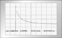
These loads can be easily integrated into the system with drivers designed for this type of load. The four high-end and eight low-end MC33888 switches from Motorola are designed to drive automotive loads. This device directly controls four high-end loads up to 60W and eight low-current loads of low current (2.5W). The MC33888 device also has built-in functionality to handle inrush currents associated with incandescent lamps. It can be seen from Figure 2 that the inrush current caused by incandescent lamps can reach 10 to 15 times the normal operating current, which causes great problems for systems without these large inrush current processing circuits. The most common measure for this type of load is to trigger an overcurrent protection circuit to cut these loads.
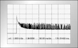
The MC33888 solves this problem well by using a start-up timer that allows the incandescent lamp to warm up before the overcurrent protection circuit works. The startup of the overcurrent protection circuit requires detection of the state and pulse width signals that regulate the output driver to the acceptable level of the device. Figure 3 shows the action waveform of the overcurrent protection. Complete battery reverse polarity protection, load dump protection and low power consumption help reduce system complexity and reduce the number of external components. Diagnostic functions include open load detection, short circuit detection, and over temperature detection. As an added protection feature, the device also has a built-in watchdog timer that can be used to shut down the device when communication between the device and the MCU is interrupted. Control of the device is achieved through a high-speed serial interface, thus greatly reducing the number of MCU pins required.
Electronic motor control
The last issue to consider is electronic motor control. The MC33887 motor driver does a good job of this task, it is a complete H-bridge driver. With a continuous current drive capability of more than 5A, the device is ideal for locking motors, antenna motors or wiper pumps. The MC33887 also features high-side current sensing feedback. The high-side current sensing feedback corrects the motor's drive frequency and duty cycle based on real-time motor current feedback. Just like a lamp driver, it automatically pulse-modulates the output when an overcurrent condition is detected.
The MC33887 device fully controls the H-bridge activation direction and load interrupt control.
Embedded emulator
Designed for complex automotive electronics applications, the MC33993, MC33887, and MC33888 devices offer advanced performance and diagnostics solutions.
Complex multi-pin MCUs often cause development problems. The MC9S12DP256 provides a single-line background debug interface that makes it easy to perform extensive debugging in an automotive environment without the difficulties common to using traditional circuit-embedded emulators. This interface can also be used to program the main flash memory at the end of the line and even to perform reprogramming operations in the car.
Modern automotive microcontrollers often use flash memory to store the main operating program. The best way to program the flash is to program the main program into the complete electronic control module after final assembly. This method can effectively avoid risks and delays compared to programming the main program into the MCU by a third party before module assembly. Time. Programming the main program into the MCU via a simple serial interface is done after the module is assembled and is typically executed during the final test. Some manufacturers use inexpensive stand-alone programmers to do this, while others integrate programming operations into test equipment at the end of the line.
Motorola's related devices provide a single-line background debug interface for flash programming, verification, and general debugging operations. When the device is operating normally, the serial communication pin is pulled high during reset, so the background system is not activated. When a programmer or debug system is connected to this pin, the pin is pulled low on reset, forcing the MCU into active background mode instead of launching the application. In order to facilitate debugging, a host system can be connected to the target MCU system during normal operation of the device, thereby monitoring the flash memory or register contents without interfering with the operation of the device. The connected debug system can also replace the MCU's control to read and write CPU registers, set hardware breakpoints, or track a single instruction.
A traditional circuit-embedded emulator typically requires between 30 and 40 connections to the target system, while the background debug interface requires only two to four connections. A single BKGD communication signal and public ground are required. Increasing the reset signal makes it easier for the host to force and control the system reset. In some cases, increasing VDD allows the debug fixture to "steal" power from the target system. This simple interface provides automotive electronics designers with the ability to debug access to MCUs installed in the sports car's electronic control module. Many problems can only be discovered when the car is traveling under normal road conditions.
Memory programming
The most important factors associated with flash programming are speed and convenience. The programming speed depends on the programming time of the flash cell and the data transfer speed from the programmer to the target MCU. Of course, there are other factors, such as the time to erase the array before programming, to verify the success of the programming operation. The MC9S12DP256 programs any 16-bit word for 45ms, but a burst programming operation allows programming of any additional word in the same bank of 32-word flashes at 20ms. In theory, the single-line background debug interface can transfer a word of information within 27ms, which is slightly slower than the actual programming time of the flash. Actual programming also requires additional task overhead, such as verification overhead. The independent programmer tool SCBDMPGMR12 can erase, program and verify 256KB of flash memory in less than 10s.
Verification is one of the important factors that generate overhead. Retransmitting all the data to achieve word-to-word verification will double the programming time. A quick way to do this is to perform a CRC calculation when the data is programmed into the flash and then reread the flash content to verify the CRC value after the entire flash programming is complete. This operation is fully possible at bus speed and there is no need to retransmit data.
Separating the data-to-target transfer so that it is completed before the data is programmed into the flash also doubles the programming time. A better approach is to extend the data transfer in parallel with the programming operation. In general, the programming algorithm is sent to the target MCU first, which facilitates management of the received data and sends the data to the RAM buffer, and then controls the erase and program operations. The programming algorithm utilizes two data buffers to receive data to be programmed into the flash. When the first buffer is full of data, the programming algorithm begins programming the data into flash and the new data is loaded into the second buffer. The background interface can be used to receive data and write them to RAM. This operation does not interfere with the operation of the target CPU because the CPU reads data from another buffer and programs it into the flash.
The flash memory in the MC9S12DP256 is divided into four independent 64KB blocks, so the erase and program operations can be performed independently on these four blocks. In the case of flash programming based on background debugging, since the data transfer speed is slightly slower than the average word programming speed of the flash memory, it is impractical to attempt to interleave the programming operation of the independent array, but perform batch rubbing on all 4 blocks in parallel. It is feasible except for the operation.
Power X (Qingdao) Energy Technology Co., Ltd. , https://www.qdpowerxsolar.com